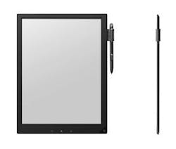
Tokyo, Japan--Sony has developed a digital-paper device based on electrophoretic technology (the same basic approach as found in the Amazon Kindle reader, whose display is made by E-Ink of Cambridge, MA, the company that first commercialized electrophoretic-display technology). Sony is aiming the device—which is 6.8 mm thick (not including the stylus holder) and has a display size of 13.3 in. (A4-paper size) and a mass of 358 g—at the academic market.
Sony says that it intends to help develop new learning and working styles in which the device is used for delivering, storing, writing, and sharing electronic files via local-area network (LAN).
The flexible electrophoretic display in the device is based on Sony’s own technology for forming thin-film transistors (TFTs) on a plastic substrate, resulting in a 1200 x 1600 pixel resolution and 16 levels of gray scale. The touch panel combines optical and electromagnetic-induction detection, allowing both touch control and writing with a special stylus pen.
The display can be used for up to three weeks per charge when the wireless LAN function is off and PDF files are viewed for at most an hour per day (including the use of the stylus for five minutes).
The digital paper can save handwritten characters, highlights, and added comments with texts, and is equipped with a microSD card slot.
Sony aims to commercialize the digital paper within fiscal 2013. Sony and Sony Business Solutions will start field tests in the latter half of fiscal 2013 by using the device in classes in cooperation with Waseda University (Tokyo), Ritsumeikan University (Kyoto), and Hosei University (Tokyo). The aim is to ultimately replace paper textbooks and learning materials with the display.
Source: http://techon.nikkeibp.co.jp/english/NEWS_EN/20130515/281531/

John Wallace | Senior Technical Editor (1998-2022)
John Wallace was with Laser Focus World for nearly 25 years, retiring in late June 2022. He obtained a bachelor's degree in mechanical engineering and physics at Rutgers University and a master's in optical engineering at the University of Rochester. Before becoming an editor, John worked as an engineer at RCA, Exxon, Eastman Kodak, and GCA Corporation.
