Forming silicon into microscopic spheres forces it to absorb infrared light, enabling better photodetectors and solar cells

March 25, 2014
A team of Spanish researchers has developed a way for silicon (Si) to absorb wavelengths in the IR that it is normally transparent to, potentially enabling more-efficient photovoltaics, as well as Si photodetectors that can function in regions of the IR that were formerly inaccessible to Si-based devices.

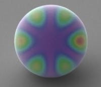
A depiction of a Mie mode is overlaid on a scanning electron micrograph of a polysilicon microsphere. (Image: UPV/CSIC)

A team of Spanish researchers has developed a way for silicon (Si) to absorb wavelengths in the IR that it is normally transparent to, potentially enabling more-efficient photovoltaics, as well as Si photodetectors that can function in regions of the IR that were formerly inaccessible to Si-based devices.1

The approach consists of shaping polycrystalline Si into microspheres that form resonators supporting so-called Mie modes, resulting in long photon dwell times and thus eventual absorption.

The researchers, from the Universitat Politècnica de València (València, Spain), the Spanish National Research Council (CSIC; Madrid, Spain), the Universitat Politècnica de Catalunya-BarcelonaTech (UPC; Barcelona, Spain) and the Universidad Rovira i Virgili de Tarragona (Tarragona, Spain), fabricated individual intrinsic Si 2.9- μm-diameter microspheres on an n-type Si substrate and measured the photoresponse, confirming the improved photoresponse.

For example, the absorption at a Mie resonance at 1245 nm was increased by more than a factor of three over a nearby nonresonant wavelength (1300 nm).

REFERENCE:

1. M. Garin et al., Nature Communications 5, No. 3440 (2014); doi:10.1038/ncomms4440
Sponsored Recommendations

Brain Computer Interface (BCI) electrode manufacturing

Jan. 31, 2025
Learn how an industry-leading Brain Computer Interface Electrode (BCI) manufacturer used precision laser micromachining to produce high-density neural microelectrode arrays.

Electro-Optic Sensor and System Performance Verification with Motion Systems

Jan. 31, 2025
To learn how to use motion control equipment for electro-optic sensor testing, click here to read our whitepaper!

How nanopositioning helped achieve fusion ignition

Jan. 31, 2025
In December 2022, the Lawrence Livermore National Laboratory's National Ignition Facility (NIF) achieved fusion ignition. Learn how Aerotech nanopositioning contributed to this...

Nanometer Scale Industrial Automation for Optical Device Manufacturing

Jan. 31, 2025
In optical device manufacturing, choosing automation technologies at the R&D level that are also suitable for production environments is critical to bringing new devices to market...

Voice your opinion!

To join the conversation, and become an exclusive member of Laser Focus World, create an account today!