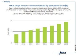
CMOS image sensor market to reach $13B by 2018, says Yole Développement
Lyon, France--Market research firm Yole Développement forecasts that the CMOS image sensor market will reach a total of $13 billion by 2018, mainly driven by consumer and automotive applications. As major technology changes (such as handset and tablet applications) continue to reshape the industrial landscape, a 10% compound annual growth rate (CAGR) is forecast for the market from 2013 to 2018.
Related: CCDs lose ground to new CMOS sensors
Yole foresees consumer applications to be the growth driver over the next five years, which is the opposite of the previous five years, which were driven exclusively by mobile applications. Moreover, after being dominated by charge-coupled devices (CCDs), digital still camera (DSC) applications are now shifting towards CMOS.
And while digital single-lens-reflex (DSLR) will be a substitution market, the next wave is likely to be automotive applications, which could become CMOS image sensors' third big market. Indeed, the CMOS image sensor market in automotive is showing steady growth, which is expected to continue in the coming years. Automotive also demands new technologies such as high dynamic range sensors and near-infrared response, and will benefit (with appropriate optimization) from technology developments in the handset market. A shift from driving assistance applications to security-based applications may imply significant quality and reliability design improvements in the near future, possibly leading to traditional automotive product providers entering the market with more exuberance.
Many other emerging applications are also set to drive CMOS image sensors' future growth, such as wearable electronics (i.e., smart watches), machine vision, security and surveillance, and medical applications. These applications are likely to be in position for strong growth in the mid- and long-term.
CMOS image sensors are undergoing numerous technological innovations. The race towards smaller pixels (thus smaller light-receiving photodiode area) to achieve better resolution also leads to pixel performance degradation due to the degradation of signal-to-noise ratio and well capacity. To cope with loss of resolution coupled with pixel size reduction, heavy process and design innovations are necessary to overcome the limitation of conventional pixel performance to move to advanced pixel technology while keeping high sensitivity.
-----
Subscribe now to Laser Focus World magazine; it's free!
