Hamamatsu to show InGaAs image sensor for NIR imaging at SPIE DSS 2014

April 15, 2014
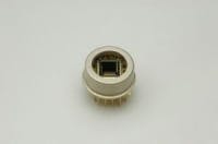
Featuring 64 × 64 pixels and 50 µm pixel pitch, the G11097-0606S is a TE-cooled indium gallium arsenide (InGaAs) image sensor that has uses in most near-infrared (NIR) imaging applications that currently use more expensive, higher density image sensors.

Featuring 64 × 64 pixels and 50 µm pixel pitch, the G11097-0606S is a TE-cooled indium gallium arsenide (InGaAs) image sensor that has uses in most near-infrared (NIR) imaging applications that currently use more expensive, higher density image sensors. Applications include thermal imaging, laser beam profiling, and NIR inspection. Its hybrid structure consists of a back-illuminated InGaAs photodiode array bump-bonded to a CMOS readout circuit. The InGaAs photodiode array is sensitive to 950–1700 nm wavelengths, with peak sensitivity at 1550 nm.

SPIE DSS booth number: 546

To Learn More:

Contact:Hamamatsu
Headquarters: Bridgewater, NJ
Product: G11097-0606S InGaAs image sensor
Key Features: 950–1700 nm sensitivity and TE cooling

What Hamamatsu says:
View more information on the G11097-0606S InGaAs image sensor.

View More Products
Locate a vendor or system integrator in our Buyer's Guide.

Share new products that you think are particularly interesting or helpful by contacting Lee Dubay, Associate Editor, Laser Focus World.
Sponsored Recommendations

Brain Computer Interface (BCI) electrode manufacturing

Jan. 31, 2025
Learn how an industry-leading Brain Computer Interface Electrode (BCI) manufacturer used precision laser micromachining to produce high-density neural microelectrode arrays.

Electro-Optic Sensor and System Performance Verification with Motion Systems

Jan. 31, 2025
To learn how to use motion control equipment for electro-optic sensor testing, click here to read our whitepaper!

How nanopositioning helped achieve fusion ignition

Jan. 31, 2025
In December 2022, the Lawrence Livermore National Laboratory's National Ignition Facility (NIF) achieved fusion ignition. Learn how Aerotech nanopositioning contributed to this...

Nanometer Scale Industrial Automation for Optical Device Manufacturing

Jan. 31, 2025
In optical device manufacturing, choosing automation technologies at the R&D level that are also suitable for production environments is critical to bringing new devices to market...

Voice your opinion!

To join the conversation, and become an exclusive member of Laser Focus World, create an account today!