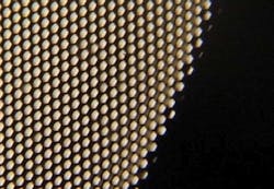
Jenoptik to show deep-UV CaF2 homogenizers at Semicon West
Jena, Germany--At Semicon West (July 10-12, 2012, San Francisco, CA), Jenoptik will be demoing new light homogenizers made of calcium fluoride (CaF2), intended for use in deep-UV photolithographic systems. The company chose CaF2 over other optical materials (a list of which is actually very short, consisting mainly of one substance—silicon dioxide in the form of fused silica) because CaF2 has a higher damage threshold and thus better longtime stability of optical performance, says Jenoptik.
Homogenizers, such as microlens arrays or diffractive optical elements (DOEs), are used in lithographic optical systems for semiconductor and flat-panel-display manufacturing, as well as inspection equipment (such as wafer, mask, and panel inspection systems). Homogenizers play a prominent role in illumination systems and create a well defined distribution of light over a particular area in a certain plane of the optical beam path. For example, very uniform intensity at the wafer plane of a lithographic system is crucial for achieving uniformity in feature size across a silicon wafer die.
The optical and micro-optical components in homogenizers have to meet requirements for a long life time and optimum transmission for short-wavelength, high-energy laser radiation.
Jenoptik is demonstrating its manufacturing capabilities for micro-optical structures in CaF2, especially for wavelengths in the range of 193-266 nm, and is exhibiting various CaF2 homogenizer arrangements. Using a microstructuring process combined with gray-scale technology and a wafer-level etching process, Jenoptik says it can fabricate customized refractive, diffractive, and hybrid structures even with asymmetric shapes and radii. The advantage of this fabrication process, according to Jenoptik, is the generation of free geometries, as well as the accuracy and reproducibility of the microstructuring process. This enables a variety of beam-distribution patterns, opening up new technical approaches where system performance of semiconductor manufacturing equipment needs to be optimized.
In addition, the company says that standard manufacturing processes are available for a range of different optical materials such as SiO2, GaAs, GaP, Al2O3, ZnS, ZnSe, Ge, chalcogenide, and others. Qualified testing at operating wavelength guarantees the quality of optical product properties, notes Jenoptik.
About the Author
John Wallace
Senior Technical Editor (1998-2022)
John Wallace was with Laser Focus World for nearly 25 years, retiring in late June 2022. He obtained a bachelor's degree in mechanical engineering and physics at Rutgers University and a master's in optical engineering at the University of Rochester. Before becoming an editor, John worked as an engineer at RCA, Exxon, Eastman Kodak, and GCA Corporation.

