400 fJ/bit silicon ‘transmitter’ uses all CMOS processes

Dec. 1, 2009
Researchers at Sun Microsystems Physical Sciences Center (San Diego, CA), Sun Laboratories (Menlo, Park, CA), and Luxtera (Carlsbad, CA) have built the lowest-energy-per-bit silicon (Si) communications transmitter (modulator plus driver circuits) to date using all complementary metal-oxide semiconductor (CMOS) processes.

Researchers at Sun Microsystems Physical Sciences Center (San Diego, CA), Sun Laboratories (Menlo, Park, CA), and Luxtera (Carlsbad, CA) have built the lowest-energy-per-bit silicon (Si) communications transmitter (modulator plus driver circuits) to date using all complementary metal-oxide semiconductor (CMOS) processes.

Click here to enlarge image

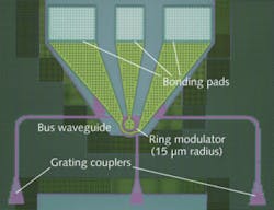
The key elements of an energy-efficient Si-based interconnect for inter- and intra-chip optical communications are a low-power modulator, a low-power driver circuit, and efficient integration of these two components. For the modulator, the researchers fabricated a ring resonator (15 µm in radius) using the Luxtera-Freescale 130 nm silicon-on-insulator (SOI) CMOS process, with grating couplers used for the optical input and output ports with surface-normal coupling. The modulator was then integrated with a separate driver circuit fabricated in its own CMOS process using flip-chip integration. The hybrid assembly was die-attached and wire-bonded to a printed circuit board and placed on a heat sink for thermal stability. Using an off-chip laser source, stable error-free transmission with a bit-error rate lower than 10-15 at a data rate of 5 Gbit/s was achieved with a power consumption of 1.95 mW, representing a record-low energy consumption of less than 400 fJ/bit. Contact Ashok Krishnamoorthy at [email protected].
Sponsored Recommendations

Brain Computer Interface (BCI) electrode manufacturing

Jan. 31, 2025
Learn how an industry-leading Brain Computer Interface Electrode (BCI) manufacturer used precision laser micromachining to produce high-density neural microelectrode arrays.

Electro-Optic Sensor and System Performance Verification with Motion Systems

Jan. 31, 2025
To learn how to use motion control equipment for electro-optic sensor testing, click here to read our whitepaper!

How nanopositioning helped achieve fusion ignition

Jan. 31, 2025
In December 2022, the Lawrence Livermore National Laboratory's National Ignition Facility (NIF) achieved fusion ignition. Learn how Aerotech nanopositioning contributed to this...

Nanometer Scale Industrial Automation for Optical Device Manufacturing

Jan. 31, 2025
In optical device manufacturing, choosing automation technologies at the R&D level that are also suitable for production environments is critical to bringing new devices to market...

Voice your opinion!

To join the conversation, and become an exclusive member of Laser Focus World, create an account today!