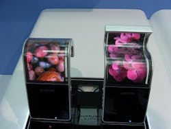
Samsung unveils high-res cell-phone-sized flexible OLED display
Chiba City, Japan--Samsung Mobile Display (SMD; Seoul, South Korea) has developed a 4.5-in. flexible organic-LED (OLED) display panel that can be bent to a curvature radius of 10 mm; the company unveiled the display at FPD International 2010/Green Device 2010.
The panel has a pixel count of 800 x 480 (WVGA)--equivalent to that for displays used in existing smart phones and mobile phones. SMD's previous version had a size of 6.5 inches and a pixel count of 480 x 272.
The new display is 240 microns thick. Low-temperature-polysilicon thin-film transistors (TFTs) were fabricated on a polyimide substrate. The organic EL elements are a top-emission type, meaning that light is extracted in the direction opposite to the TFT substrate. Low-molecular-weight red, green, and blue light-emitting materials were applied by using vapor deposition.
The brightness and contrast ratio of the display are 250 cd/m2 and 100,000:1, respectively. It can display about 16.7 million colors and has a 100% or higher color gamut on NTSC standards. The release date of the panel has not yet been decided.
source: Tech-On
Subscribe now to Laser Focus World magazine; it’s free!

John Wallace | Senior Technical Editor (1998-2022)
John Wallace was with Laser Focus World for nearly 25 years, retiring in late June 2022. He obtained a bachelor's degree in mechanical engineering and physics at Rutgers University and a master's in optical engineering at the University of Rochester. Before becoming an editor, John worked as an engineer at RCA, Exxon, Eastman Kodak, and GCA Corporation.
