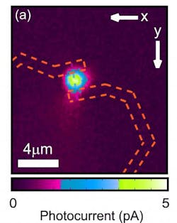
Delft and Eindhoven, The Netherlands--Moving a step closer toward quantum computing, a research team in the Netherlands has fabricated a photodetector based on a single nanowire, in which the active element is a single quantum dot with a volume of a mere 7000 nm3. The team was made up of researchers from the Delft University of Technology and Philips Research Eindhoven.
Photodetectors based on single quantum dots are expected to find uses in optoelectrical interfaces in future quantum computers, where single photons will carry information over long distances and single electrons will be used for computation.
"Our research team fabricated a very localized light detector with dimensions far below the wavelength of light, which enables detection with very high spatial resolution," said Val Zwiller of the Kavli Institute of Nanoscience at Delft University of Technology.
"In addition, because quantum dots have discrete energy levels, only light in resonance with the energy levels of the quantum dot will be detected. The indium phosphide nanowire was grown with standard epitaxial techniques and the quantum dot was obtained by sandwiching a thin segment in between with a lower bandgap. We created the device using electron-beam lithography to contact a single nanowire."
The detectors have a quantum efficiency of 4%, which is good for a nanodevice.
REFERENCE
1. M. P. van Kouwen et al., Applied Physics Letters, 97, 113108 (2010); doi:10.1063/1.3484962.
Subscribe now to Laser Focus World magazine; it's free!

John Wallace | Senior Technical Editor (1998-2022)
John Wallace was with Laser Focus World for nearly 25 years, retiring in late June 2022. He obtained a bachelor's degree in mechanical engineering and physics at Rutgers University and a master's in optical engineering at the University of Rochester. Before becoming an editor, John worked as an engineer at RCA, Exxon, Eastman Kodak, and GCA Corporation.
