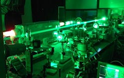
Scientists from Tomsk Polytechnic University (TPU; Tomsk, Russia) together with colleagues from the E.V. Zuev Institute of Atmospheric Optics SB RAS (IAO SB RAS) are designing an advanced laser monitor that enables observing high-speed processes hidden by powerful illumination. A simple example of such processes is welding. Previously, the research team developed a monitor prototype based on a single laser. Now, they are developing a two-laser monitor. This will make it possible to obtain better images and even to observe X-ray processes.
RELATED ARTICLE: Flame spectrometers quantify volcano emissions
The creation and analysis of new, high-energy materials and processes is often accompanied with powerful, fiery illumination that makes process monitoring difficult. There are two active components within the monitor: two lasers. The first one highlights an object or process under study, while another filters the illumination and enhances the resulting image.
"Two lasers help us to overcome some restrictions of a monostatic laser monitor where one laser is used. For instance, they increase a limit distance. This is the biggest distance for observing the process. A single laser monitor operates at up to three meters. There are also processes with both background illumination and X-Ray radiation that can disable electronics. A bistatic laser monitor with two lasers will allow us to move away from an object for dozens of meters and to visualize complex processes," says Maxim Trigub, an associate professor of the TPU Department of High-Voltage Electrophysics and High-Current Electronics, a research fellow of IAO SB RAS.
The new version of the monitor provides for more contrast images of objects and enhances the system's vision. "Enhancing view area means that at a certain distance we can see a larger area of the object than before," clarifies the researcher.
The development is relevant, first of all, for welding and foundry industries. A number of scientific institutions are interested in it as well. "A working single-laser prototype has already been used for joint research by the Institute of Strength Physics and Materials Science SB RAS and the Institute of Electrophysics UB RAS," says the project participant Nikolay Vasnev.
SOURCE: Tomsk Polytechnic University; https://tpu.ru/en/about/tpu_today/news/view?id=1841

Gail Overton | Senior Editor (2004-2020)
Gail has more than 30 years of engineering, marketing, product management, and editorial experience in the photonics and optical communications industry. Before joining the staff at Laser Focus World in 2004, she held many product management and product marketing roles in the fiber-optics industry, most notably at Hughes (El Segundo, CA), GTE Labs (Waltham, MA), Corning (Corning, NY), Photon Kinetics (Beaverton, OR), and Newport Corporation (Irvine, CA). During her marketing career, Gail published articles in WDM Solutions and Sensors magazine and traveled internationally to conduct product and sales training. Gail received her BS degree in physics, with an emphasis in optics, from San Diego State University in San Diego, CA in May 1986.
