Breakthrough material for broadband photodetectors: Gii
When was the last time you thought about broadband photodetectors? A small but mighty piece of technology, broadband photodetectors are optoelectronic devices that convert electromagnetic waves into electrical signals. Unlike conventional photodetectors, which are limited to a narrower range of wavelengths, broadband photodetectors detect a broad spectrum, typically covering ultraviolet (UV) to infrared (IR) light, encompassing the visible spectrum.
Broadband photodetectors are essential in numerous applications due to their ability to detect multiple wavelengths within the electromagnetic spectrum. In telecommunications, they play a crucial role in fiber-optic networks by converting light signals, which carry vast amounts of data, into electrical signals for processing and transmission. In medical imaging, these photodetectors enable advanced techniques such as optical coherence tomography (OCT) and IR imaging, which provide detailed images of tissues and improve diagnostic accuracy. Their versatility also makes them valuable in environmental monitoring, spectroscopy, and scientific research, where broad wavelength detection is necessary.
In short: broadband photodetectors are one of the millions of essential components that make our world go around. And they’ve been a focus of our research for several years. While these devices have advanced significantly, our recent study marked the first time we tested a fascinating new material called “Gii.”
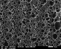
We learned about it through the broader Scottish academic ecosystem. Developed by Scotland-based iGii, Gii is a sustainable carbon nanomaterial that can be engineered at an industrial scale without mining or high energy, which are both toxic processes. Gii was previously tested for a number of different use cases, such as self-powered sensors, energy harvesting devices, and energy catalysis.1
We knew it had a number of desirable properties—including great optical absorption and excellent electrical conductivity—that boost the responsivity and external quantum efficiency (EQE) of the photodetector within a wide spectral range, so we wondered what would happen if we used it as a broadband photodetector.
Proof-of-concept study
Our research was the first proof-of-concept study of Gii within broadband photodetectors. We explored its optical and structural properties to assess its viability by focusing on two types: standard Gii (ST-Gii) and low-resistance Gii (LR-Gii).
Using Raman spectroscopy, a technique to measure the interaction of light with molecular vibrations (scattering), we analyzed Gii samples placed onto a thin, flexible Kapton substrate. We tested samples with different laser wavelengths—455, 532, 663, and 780 nm—under varying power conditions (1 to 8 mW) to evaluate their responses.
Gii absorbs the full spectrum of light
We found Gii to be an exceptional material capable of absorbing the full spectrum of light—from UV (380 nm) to IR (750 nm)—because of the material’s properties. There is no need to treat its surface with external photosensitive materials.
The ability to capture a broad spectrum of light makes broadband photodetectors useful. In telecommunications, it allows the simultaneous detection of different light signals, which improves data transmission capacity and efficiency. In medical imaging, detecting a wide range of wavelengths enables techniques like multispectral and hyperspectral imaging, which provide more detailed and accurate diagnostics. For environmental monitoring, it facilitates the detection of various pollutants and gases that absorb light at different wavelengths.
In scientific research and spectroscopy, broad wavelength detection is essential for analyzing materials and phenomena that exhibit complex spectral characteristics, which leads to more comprehensive and precise measurements.
Gii’s ability to do this via a single material makes it a superior candidate for broadband photodetectors, which often require multiple materials to achieve the same functionality. Using a single material reduces costs, improves reliability, and enables more compact designs.
Demonstrated optical switch behavior
Notably, we identified Gii’s optical switch behavior. This property allows the material to produce varying amounts of electric charge depending on the light wavelength used, which enables applications in telecommunications, optical signal processing, and data centers.
Gii also exhibited a high surface-to-volume ratio, which makes it more sensitive toward UV or IR ranges through the use of quantum materials. This feature has potential not just for broadband photodetectors, but for energy storage devices and also as a platform for hosting quantum sensing materials, such as quantum dots.
Challenges
One of the key challenges of using Gii’s optical switch behavior for practical devices is understanding and controlling how its vibrations (phonons) interact with its electrical properties (electrons).
While Raman scattering provided evidence of this interaction, measuring it with conventional light sensors, such as photodiodes, is difficult because defects within these sensors—called traps—cause electrons to lose energy before their behavior can be fully captured. We’re currently running further experiments to explore ways to overcome this limitation by testing Gii under different light conditions and analyzing these traps. Our ultimate goal is to translate the advanced Raman-based findings into a portable chip and to pave the way for real-world applications.
Applications and timeline
The practical applications for this technology are vast and there is plenty of scope to explore more “proof of concepts” of Gii within the field of optoelectronics.
Our research is exploring combining Gii with quantum dots to broaden photon detection, and form the basis for developing an electronic cloth for telemedicine applications. It’s a really exciting project and we look forward to sharing our findings during the years ahead.
FURTHER READING
E. Keel, M. Caffio, D. Gibson, and C. Garcia Nuñez, Proc. SPIE Photonics Europe, 13015, 1301513 (Jun. 18, 2024); https://doi.org/10.1117/12.3017247.
REFERENCE
- E. Keel et al., Nano Energy, 112, 108475 (2023); https://doi.org/10.1016/j.nanoen.2023.108475.
About the Author
Des Gibson
Des Gibson is a professor of thin film and sensor technologies at the University of the West of Scotland Institute of Thin Films, Sensors & Imaging.
Carlos Garcia Nuñez
Carlos Garcia Nuñez is a lead academic in the area of semiconductor thin films and nanostructures at the James Watt School of Engineering at the University of Glasgow.

