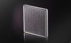
Microlens Arrays: Versatile and Efficient
Imagine integrating the power of nature’s compound eyes into a compact optical assembly just 10 mm by 10 mm. With microlens arrays, this is now possible. These arrays are ideal for homogenizing light from line-narrowed excimer lasers or high-power LEDs, delivering high efficiency and non-Gaussian uniformity. Comprising numerous tiny microlenses arranged in one or two-dimensional arrays, they revolutionize light management in various applications.
Design and Composition of Microlens Arrays
Microlens arrays can be produced as separate optical components or incorporated into larger systems. They might be mounted within metal or polymer structures for easy integration. Each array can include thousands to millions of microlenses, arranged in grids, rectangles, or circles. Key parameters such as focal length, transmitted wavefront quality, and size define their performance.
Most microlens arrays are made from UV fused silica, known for its excellent transmission from UV to IR. The fill factor, which depends on the microlenses’ geometry and arrangement, is typically high to prevent zero-order hotspots. These arrays offer a large field of view, low aberration and distortion, infinite depth of field, and high temporal resolution, making them indispensable in various fields.
