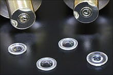
Process Metrology Helps Ensure Quality of Smartphone Camera Lenses
With approximately 40 million micro lenses manufactured every day, there is an increasing demand for fast, high-quality, reliable metrology to support this scale of precision manufacturing. As cameras increase in image quality, tolerances of lens designs become tighter, and characterization requirements become broader. To gain a sense of the metrology requirements, and how the ZYGO's Compass™ micro lens metrology system can meet these requirements, we need to look at the manufacturing process.
How Smartphone Micro Lenses are Made
Before a micro lens can be manufactured, a metal lens mold must be diamond-turned to a specific aspheric shape with tight dimensional tolerances. Two molds are required for each lens design, corresponding to Side 1 and Side 2 of the lens. Once the molds are cut, they are brought together, creating a cavity. Optical grade plastic is injected into the cavity, forming a plastic micro lens. Typically, each camera lens module requires 4 to 6 lenses of unique design. These lenses are then assembled into a stack and become the heart of the camera lens module.
Metrology of In-Process Micro Lenses
The Compass™ micro lens metrology system provides lens verification through the measurement of micro lenses and lens molds, and does so without contacting the surface of the samples being measured – completely avoiding any potential for damage. It can help to standardize and streamline the verification process, providing full characterization of highly-precise micro lenses, and does it in a fraction of the time of competing systems.
One System – Multiple Measurement Types
The system's custom multi-axis staging allows for characterization of a wide variety of lens designs, with complex geometries, without sacrificing measurement accuracy. And ZYGO's proprietary Mx™ software provides a full suite of measurement results which would typically require 2 or 3 conventional metrology instruments to replicate. By reducing the number of tools in the inspection process, less time is spent on operator training. Additionally, one Compass™ system may replace multiple conventional instruments thus freeing up valuable floor space in a manufacturing facility.
Catching Defects, and Gaining Process Insight
Not only does the Compass™ system feature a broad range of capabilities, it is actively solving industry problems. Increasingly complex camera designs require complex surface geometries such as gullwing, bathtub, high-slope concave and convex style lenses. While these present a challenge for both manufacturing and conventional metrology, the Compass™ system can characterize all these types of surfaces without compromising precision or accuracy. Through full-surface 3D metrology, the Compass™ system can identify defects that would otherwise be missed, which would be detrimental to lens performance and image quality. Identifying and quantifying them can give manufacturers valuable insight about their processes.
The Right System for Now, and for the Future
The rapid growth of micro lens technology in consumer electronics requires a metrology instrument that works at the speed of the industry. The Compass™ system has set the standard for micro lens metrology systems that measure deviation and process asymmetries with ease. Products will only grow more complex, so having a versatile, precise, and powerful surface metrology system available is integral to be ready for whatever is next in micro lenses.
