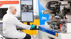
Bay Photonics Targets Fine Pitch Placement of Flip-Chip Photonics Devices Utilizing Palomar 3880 Die Bonder
Carlsbad, CA – February 4, 2021 – Palomar Technologies, a global leader in delivering total process solutions for advanced photonics and microelectronic device packaging, announced today that Bay Photonics is working on projects that require the placement and bonding of flip-chip photonics devices that require the use of specialized equipment and are using a Palomar 3880 Die Bonder in the process.
Bay Photonics, a UK-based company specializing in advanced photonics assembly and packaging is involved in the prototype development stage of projects requiring fine pitch of hundreds of bonding pads, some at 60-micron level. The Palomar 3880 die bonder recently purchased by EPIC Paignton is being utilized to ensure that the final layout of the photonic ICs (PICs) is suitable for the targeted assembly and packaging processes.
Glenn George, Managing Director of Bay Photonics commented: “I am particularly pleased that prospective customers have contacted us to help with these highly accurate PIC assembly and packaging projects. It’s exciting to see that the idea of creating a hub for Photonics development at EPIC is working, not only from Bay Photonics perspective of moving to this fantastic building, but also involving the eco-system that EPIC brings, using machinery that Palomar have commissioned and the willingness of EPIC and Palomar Technologies to help accomplish these advanced photonics technology requirements.”
Bay Photonics founded with former employees of Nortel/Bookham, Gooch & Housego, and Eltek Semiconductor have a deep understanding of the capabilities are of the various assembly methods for specific photonics applications and how to use that knowledge for building commercial prototypes that could transition to production volumes if so desired.
Josef Schmidl, Managing Director EMEA for Palomar Technologies said, “We are thrilled to work closely with Bay Photonics, particularly in this area of advanced photonics packaging. Today’s photonics applications are becoming extremely complicated and with our vision to create simple solutions for complex processes, we are dedicated to finding solutions for our customers. Our focus in placing our equipment with EPIC is to enable our customers to realize the high growth potential opportunities that are available in these exciting, rapidly evolving industry sectors.”
About Palomar Technologies
Palomar Technologies makes the connected world possible by delivering a Total Process Solution™ for advanced photonic and microelectronic device assembly processes utilized in today’s smart, connected devices. With a focus on flexibility, speed and accuracy, Palomar’s Total Process Solution includes Palomar die bonders, Palomar wire and wedge bonders, SST vacuum reflow systems, along with Innovation Centers for outsourced manufacturing and assembly, and Customer Support services, that together deliver improved quality and yield, reduced assembly times, and rapid ROI.
With its deep industry expertise, Palomar equips customers to become leaders in the development of complex, digital technologies that are the foundation of the connected world and the transmission of data generated by billions of connected devices. Palomar solutions are utilized by the world’s leading companies providing solutions for datacom, 5G, electric vehicle power modules, autonomous vehicles/LiDAR, enhanced mobile broadband, Internet of Things, SMART technology, and mission-critical services.
Headquartered in Carlsbad, California, Palomar offers global sales, service and application support from its offices in the USA, Germany, UK, Singapore, and China. For more information, visit: http://www.palomartechnologies.com.
About Bay Photonics
Bay Photonics are an independent Photonics IC (PIC) assembly and packaging company. Helping innovative projects from the research/bread board stage through to volume production. Academic and commercial projects accepted.
They specialize in helping build prototypes that require a flexible and technically innovative approach to package design, assembly and test of devices. Designs requiring single fibre(s), fibre arrays and micro-optics are our specialty. Having worked at world leading opt-electronic component manufacturers, our technical team have vast experience in developing the right packaging and production solution for PICs in various applications including datacom, quantum and medical amongst others.
Located in the South West of the UK, with our main office in Paignton at the Electronics & Photonics Innovation Centre (EPIC), we are housed with other members of the Torbay Photonics Cluster ecosystem and together, offer extended expertise and capability. www.bayphotonics.com, email: [email protected].
About the Electronic and Photonics Innovation Centre (EPIC)
EPIC is managed by TDA, a trading name of Torbay Economic Development Company Limited. As a Centre of Excellence, EPIC will provide the ideal environment for both small and large technology companies within the sector. The Centre will provide opportunities for collaboration, R&D, design, new product development. The facility has established links with academia and research institutes, and other European clusters as well as looking to develop global partnerships. Companies wishing to benefit from the world class facilities at the White Rock site should contact the Centre Director Wayne Loschi on [email protected]. For more information, visit: https://epic-centre.co.uk/
