Measuring Surface Form of Thin Plane-Parallel Optics, the Quick and Easy Way
Measuring the surfaces of thin, plane-parallel optics has been historically problematic because the front and back surfaces are so close together. Multiple reflective surfaces in close proximity make it very difficult – if not impossible – for standard interferometry techniques to obtain reliable measurements.
Why is it Difficult?
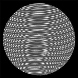
When trying to measuring thin optics with traditional phase-shifting interferometry (PSI), a second reflection is returned to the interferometer from the back surface of the optic. This results in multiple overlapping interference fringes resulting in a complex pattern (shown in the image above) that PSI cannot accurately analyze.
Shortfalls of Traditional Methods
Several work-around methods have been developed to overcome the fundamental limitations of measuring thin plane-parallel optical components with PSI, such as coating the back surface with materials that reduce or eliminate the secondary reflection. Applying black paint, coloring with a dark marker, or spreading petroleum jelly on the back surface takes time, adds undesirable steps to the metrology process, and carries the risk of damaging or distorting a thin component when applying or removing the coating.
ZYGO Patented Technology Makes It Quick and Easy
Fortunately, ZYGO's innovative engineering staff developed (patented) technologies to distinguish each surface of a thin plane-parallel optic, and characterize the quality of both in a single measurement, even for components thinner than 1 millimeter.
Bonus: Homogeneity and Thickness Variation Measurement
An important property of an optical component is the homogeneity of the refractive index of the material from which it is made. Variations in the material's refractive index affect the wavefront passing through it, thus potentially affecting the performance of the optic in critical applications. Similarly, variations in the thickness of the optic alter the length of the optical path, which can also adversely affect the wavefront.
The capability to measure optical homogeneity and total thickness variation (TTV) is a standard feature of ZYGO's Verifire™ MST laser interferometer system. A simple, two-measurement process is all it takes. Traditional methods, involving the use of oil-on plates, or requiring the optic to have a degree of wedge, are no longer necessary.
Learn More About It
For a more in-depth look at the measuring multiple surfaces of thin optical components, download the technical article How to Measure Thin Parallel Optics.


