Carlos Lee: What’s the backstory behind you becoming CEO of VTEC?
Jan Mink: Prior to setting up VTEC, I spent most of my life at Philips Electronics. I started in 1977 working on passive components, and in 1979 I moved into semiconductor laser development using scanning electron microscopy for in-process failure analysis.
In 1985, while working full-time with Philips, I graduated from Eindhoven University of Technology with a MSc in physics. I was then promoted to manager of Philips Optoelectronics’ R&D department, where I was responsible for all R&D, the testing activities, and quality control of their photonics products.
In 1998, I became R&D manager for consumer electronics—flat-screen TVs, audio equipment, and entertainment.
In 2000, I and four others cofounded a subsidiary of a Californian startup, Genoa BV, in Eindhoven, with me as managing director. The idea was to focus on linear semiconductor optical amplifiers for metro applications, building on the knowledge we had of similar devices made at Phillips.But two years later, with the collapse of the photonics economy, the startup folded, and I rejoined Philips Electronics as leader of the Sensors and Measurements group. In 2004, Philips started to restructure and cut back on all kinds of activities and, although I was still technically working for Philips, they allowed us to set up our own company: 2M Engineering.
The aim was to use our expertise in sensors to develop applications in the areas of medical devices and industrial and environmental IoT solutions. In 2011, I sold my shares and set up VTEC as a separate entity.
CL: How has the company evolved?
JM: From the outset at VTEC, our aim wasn’t to follow the traditional business model by having a line of products or to offer specific services to customers. Instead, our goal was to use our analysts, designers, and technicians together with our own production facility in Shanghai to provide a one-stop shop to create customized solutions for manufacturing, health and fitness, education, communications, and a wide variety of other industries.
These solutions are based on the two pillars of photonics and IoT, and our work focuses on three main areas. First, to develop the technology and secure funding by participating in various Dutch and international projects, such as Fodamed, Misca, and OIP4NWE; secondly, to develop products in both pillars, based mainly on sensors for domestic, industrial, and medical applications, applying technologies like magnetic encoders, lasers, and photonic integrated circuits; and thirdly, to provide consultancy to help customers develop their applications.
We currently have a workforce of around 15 who, together with student interns, can cover all the requirement skills, including sensor design, sensors, electronics design, embedded design, and wireless and other types of communication. We are also working in the cloud and perform data analysis all the way down to machine learning and artificial intelligence.
CL: What are the main advantages and challenges of being on your own?
JM: The main advantage is that as I don’t have any investors, I can make my own decisions and choices and I don’t need to tell anybody what I've done or plan to do. Of course, it’s totally different working in a big company that’s looking for big investments. Then, you have to prepare proposals and convince your bosses and/or the investors. To do this, you have to be a special type of person, which is not really my strength.
Regarding technical challenges, doing photonics requires a wafer fab, and because that’s not something we can do ourselves, it’s been a challenge to find a wafer fab that can provide the devices we design at the right quality and at the right time.
Another challenge is managing cash flow—finding different ways to ensure money is in the bank at the end of the month to pay employees.
A more recent challenge is since I only have a few Dutch employees, during and after COVID a lot of my staff went back to their home countries to look for a more comfortable and secure job. But this has been offset by hiring new employees and, to some degree, the 10 interns who join us every summer from Strasbourg to do small photonics projects ranging from electronics to measurements and building setups for simulations.
CL: What do you envision for the future?
JM: In the Netherlands, there are now many programs for post-COVID recovery, so there’s a lot of potential growth from these funds.
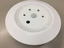
I expect sensors to contribute to a much bigger chunk of turnover, especially with an office sensor we’ve developed to monitor up to 10 parameters for use within the fast-growing smart buildings market.As far as photonics, we’ve also applied to participate in a project to develop receivers and transmitters for free-space optical communication. I’ve also solved the wafer fab problem, so we now have multiple possibilities to create a wide range of different products with short throughput times and high process quality.
CL: What’s your advice for the next generation of entrepreneurs?
JM: The first thing is to decide what kind of company you would like and what kind of businessperson you want to be. If you want to make money quickly and you are sales-oriented, you will need to start reselling products, which means finding the right products and the right customers.
On the other hand, if you’re more of a technical person and you want to develop a technology, it will take a lot longer to make money and you will need to be patient because it can take a long time for projects to develop, at least to the level where you can be considered a solid company.

Carlos Lee
Carlos Lee is Director General of the European Photonics Industry Consortium (EPIC; Brussels, Belgium), an active industry association that fosters a dynamic photonics ecosystem by maintaining a strong network and acting as a catalyst and facilitator for technological and commercial advancement.


