Achieving higher functionality per unit chip area has driven the VCSEL industry for the last 20 years. TRUMPF’s industrial-grade approach for long-wavelength VCSELs enables the direct combination with the other technical building blocks it’s already developed, including polarization stabilization and integrated lenses. By surpassing the longer wavelengths’ brick wall, many more features should be accessible soon.
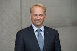
Read on as I discuss long-wavelength VCSELs with Berthold Schmidt, CEO at TRUMPF Photonic Components.
Laser Focus World: What’s been the driving force in developing long-wavelength VCSELs for high volume applications?
Berthold Schmidt: Long-wavelength VCSELs, like so many other laser applications, have been waiting for a while to find a right field of use, which would justify major investments in this technology. Nowadays, we are seeing increasing interest from a variety of industries in small, compact light sources. There is, for instance, the consumer electronics industry: OLED displays have a transmission window in the range of 1350 to 1480 nm. Sensors in this wavelength regime supporting flood illumination, dot pattern, time-of-flight (ToF), and indirect time-of-flight (iToF) functions can be easily placed below the display without disturbing other functionalities and with the benefit of higher eye-safety standards. Our technology aims to support that. But there are also other fields that benefit from lower-cost SWIR light sources. Applications in datacom, telecom, and LiDAR are prominent examples, to name just a few. Moreover, the technology can be easily extended to wavelengths of up to ~2000 nm, allowing, for instance, a wider variety of products to be offered to the industrial sensor market.
LFW: There are always potential benefits to being the first to market with an innovative offering. What do you see as the keys to a successful launch for this technology?
BS: We didn’t aim to reinvent long-wavelength VCSELs, as they have already been in the market for more than 20 years. But from the very first day, we focused on establishing a high-volume process on a larger wafer scale produced on industrial-grade III-V equipment and therefore capable of good yield levels. The fact that the performance and robust nature of these devices is exceptional is a consequence of the thorough development approach our engineering team took.
Successful industrialization of VCSEL technology is often initiated by demands for lower cost and miniaturization at high volume. While traditional markets for long-wavelength VCSELs, such as telecom and industrial sensing, haven’t provided the leverage for high investments, we consider the future demand in consumer sensing, LiDAR, photonic integrated circuits (PICs), and quantum photonic integrated circuits (QPICs) as promising candidates to finally enable that.
LFW: Any surprises or lessons learned throughout the development process?
BS: Many! I’m always astonished to see how vigorously the equipment industry has evolved during the past two decades. Processes that we considered complex and thus impossible are suddenly standard due to significant investments, mainly in the silicon industry, of course. This new dimension of process options opens new pathways to more solid and therefore industrial-grade manufacturing for III-V photonic components in the long-wavelength regime.
LFW: Any remaining obstacles that could hamper deployment into the high-volume applications you are pursuing?
BS: The groundwork for long-wavelength VCSELs in high volumes has been made. But this is a capex-heavy industry. New investment in production equipment is necessary to roll out devices in large volume. What’s more, commercial success also depends on quick yield improvements and standardization. Customer commitments are therefore required to dedicate the fabrication and testing to the defined wavelengths and specifications. This is key for reducing costs and realizing the true potential of this technology.
About the Author
Peter Fretty
Vice President, Market Leader, Digital Infrastructure
Peter Fretty began his role as the Vice President, Market Leader, Digital Infrastructure in September 2024. He previously served as Group Editorial Director for Laser Focus World, Military & Aerospace Electronics and Vision Systems Design, and as Editor in Chief of Laser Focus World from October 2021 to June 2023. Prior to that, he was Technology Editor for IndustryWeek for two years.
As a highly experienced journalist, he has regularly covered advances in manufacturing, information technology, and software. He has written thousands of feature articles, cover stories, and white papers for an assortment of trade journals, business publications, and consumer magazines. He has also owned and operated numerous manufacturing companies.

