A big vision comes to life: Optical interconnects for AI
As a child, Mark Wade was fascinated by astronomy, often staring up at the night sky, pondering questions about the cosmos; the stars and the moon motivated him to seek answers. This attraction to solving the unknown propelled him to study physics, where he felt as though he was uncovering the rules to the secrets of the universe. Little did he know at this early age, he would someday solve a future mystery: how to keep up with the speed of artificial intelligence (AI).
Roots in education and research
As Wade grew, so, too, did his curiosity. He attended Louisiana Tech University to gain undergraduate degrees in physics and electrical engineering. He became “hooked” early on, pushing to learn and discover more, so it came as no surprise that Wade decided to pursue higher education. While visiting graduate schools, he first heard about silicon photonics and became a photonics devotee.
Jumping right in, Wade attended the University of Colorado Boulder for his master’s and Ph.D. in electrical engineering. He realized the world of photonics was poised to have a significant impact on computing, and he was able to participate in many projects with breakthrough results—including building the first-ever CPU-to-memory photonics interconnects. Early success fed his belief in the power of photonics, and he became an MIT research affiliate.
At MIT, Wade was part of a collaboration exploring ways data transmission could keep up with Moore’s law—and the team struck gold. The core breakthrough was fast and efficient optical technology built into existing silicon chip design to replace the copper wires. This new chip design not only improved efficiency in input/output (I/O), but, importantly, reduced energy consumption because the photonic integration produced very little heat waste. This energy breakthrough led him and his colleagues to submit their design to an MIT clean energy competition—and they won.
From research to reality—with a different approach
Confidence from that win and a pocketful of prize money inspired them to get started, and Wade and colleagues realized the best way to accelerate progress and bring the lab results to real life was to launch a company. In 2015, while still students, Ayar Labs (formerly OptiBit) was born.
After graduation and relocating to the San Francisco Bay area, the team began the demanding work of taking their technology from the lab to a commercially viable device. They began simultaneous rounds of R&D, funding, and broad ecosystem development.
As product development took shape, Wade and his team approached the problem from a different angle than the rest of the industry. Instead of working solely to build an optical device, they concentrated on solving the computing pain point. The team was future-focused on what computing systems would look like and how computing systems would need to scale in terms of performance. For computing, it was clear there was not only an optical device problem, but a system problem that funneled down to the device.
With this future focus as their guide, the team bet big on AI as a massive opportunity. Wade believed AI infrastructure would need optical I/O to scale performance and alleviate the data bottleneck to avoid hindrance on AI performance and potential. Part of this opportunity, he believed, was the paradigm shift happening with chips. He recognized that an optical I/O chiplet would need to exist in standard ecosystems and it would be the key to enabling AI.
Collaboration in the high-volume ecosystem drives results
With AI in mind, Wade knew he needed to bring together collaborators from multiple technical domains. He sought out those with expertise in high-speed circuit design, electrical signaling, semiconductor materials, process integration, and device design.
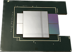
The result? Ayar Labs created an in-package optical I/O chiplet that shifts data transfer efficiency and bandwidth by connecting nodes to effectively function as one giant graphics processing unit (GPU). Product testing shows powerful results: It produces 5x higher bandwidth, 10x lower latency, and is 8x more power-efficient than standard solutions.
With the baseline product established, Wade realized a new photonics technology would ultimately become a manufacturing problem. Again, the team took to collaboration to ensure the go-to-market supply chain became a capable ally. He created partnerships with the likes of GlobalFoundries, Lumentum, Macom, and Sivers Semiconductors to alleviate anticipated pain points and solve for potential high-volume hindrances.
The future
Ayar Labs has grown by casting into the future, and as Wade considers what’s next for the organization, he began contemplating the role of optics within consumer products. He’s focused on how the present can build and evolve so the whole ecosystem moves one step at a time.
Wade observes today’s photonics landscape with a sense of possibility, looking for the next grand adventure. He sees photonics’ capabilities and performance growing a commercial user base—aerospace, cloud and data centers, high-performance computing, and telecommunications—that will prove out the next round of solutions and introduce new capabilities for mass-market manufacturing. Once it occurs, he believes many more opportunities, including consumer products, will present themselves.
Entrepreneur takeaways
Looking back on his career, Wade points to creative thinking as a lynchpin of success. In the startup phase, he and his team spent considerable time ignoring what the industry was doing and instead dove deep into their own ideas and vision. Undeterred by taking a different approach, the team is revolutionizing how photonics are incorporated into critical technologies. The takeaway? The courage to think differently makes a difference.
From a little boy dreaming of stars to a CEO powering the next round of technology, Wade has had quite the road to success, driven by his sense of curiosity and a willingness to ask: “What if?” As he considers what’s next, that same philosophy holds true: At Ayar Labs, he and the team are enjoying the journey and keeping their eyes on the horizon for what the future will hold.
About the Author
Jose Pozo
Chief Technology Officer, Optica
Jose Pozo joined Optica in March 2022, and has spent more than 25 years working in photonics. He earned a PhD in quantum physics from the University of Bristol (U.K.), and an M.Sc. and B.Eng. in telecom engineering from UPNA, Spain / VUB (Belgium). Prior to joining the European Photonics Industry Consortium (EPIC) in 2015 as CTO, Jose was a Senior Photonics Technology Consultant with PNO Consultants, with some of the main accounts such as CERN, Thales, and TE Connectivity. He has worked at TNO, The Netherlands Organization for Applied Scientific Research, and as a postdoctoral researcher at the Eindhoven University of Technology in the Netherlands, where he contributed to the early development of EFFECT Photonics.


