Photonic Integrated Circuits: Silicon-photonic-based PIC modulators scale up for dense datacenter interconnects
JIANYING ZHOU
The proliferation of mega-sized datacenters along with distributed optical communications architectures is creating high-volume demand for datacenter interconnect (DCI) coherent transmission systems that offer high capacity per channel and per fiber.
These DCI links generally cover distances less than 100 km and operate at 400 Gbit/s per wavelength using 64 Gbaud/16 QAM (quadrature amplitude modulation) or 600 Gbit/s using 64 Gbaud/64 QAM—and soon 800 Gbit/s using 90 Gbaud/32 QAM.
Coherent modulators used for these high-speed networks are complex, nested Mach-Zehnder modulators (MZMs) made using photonic integrated circuits (PICs) based on one of the following platforms: indium phosphide (InP), lithium niobate (LiNbO3), or silicon photonics (SiPho).
While each of these platforms has its advantages and disadvantages, InP and LiNbO3 generally have higher performance for modulation. However, for high-volume applications, SiPho enables cost-efficient, small-form-factor coherent modulators due to the high-yield photonic-electronic integration achieved through leveraging established large-scale silicon wafer processes for mass production, high yield, and high reliability.
The case for SiPho-based PICs
In addition to small form factors and both high yields and reliability, SiPho provides a straightforward path to higher levels of integration—and manufacturing scalability—by combining the coherent receiver with the coherent modulator in a coherent optical sub-assembly (COSA).
NeoPhotonics has developed a carrier depletion MZM-based in-phase quadrature (IQ) modulator operating at 600 Gbit/s using 85 Gbaud/16 QAM and 64 Gbaud/64 QAM.1 The device was manufactured using a commercial SiPho fabrication process and demonstrates a more-than 25 dB extinction ratio, a half-wave voltage (Vπ, or the voltage required to induce a phase change of π for the light going through the modulator) of 4 V, and an on-chip insertion loss of 7 dB.
With careful semiconductor doping and device design optimization, high-speed electrooptic response is achieved with a simple differential coplanar electrode structure. This performance level and chip size is suitable for pluggable 400ZR modules (a 400G Ethernet standard) as well as for compact 600G line cards.
SiPho modulator challenges
Silicon photonic modulator design has many more constraints than InP or LiNbO3 modulators. Most commercial SiPho modulators operate using carrier depletion, so the associated dopant level is a complex issue. A high carrier concentration can increase the efficiency of the phase shifter (PS) portion of the modulator (lower Vπ), while at the same time increasing loss. Moreover, the dopant level also affects the series resistance/capacitance and therefore the bandwidth.
These considerations are on top of the conventional design constraint on PS length and the radio frequency (RF) loss associated with the electrodes, which also applies to InP and LiNbO3 modulators: a shorter device is better for bandwidth and loss, but worse for Vπ. Therefore, there are many more counter-balancing tradeoffs for SiPho than for InP and LiNbO3 modulators.
While carrier depletion traveling waveguide Mach-Zehnder modulators (TW-MZMs) may be the most cost-efficient with all-silicon material for commercial use, the design for a high-speed, high-performance SiPho modulator is challenging, as it involves several key elements that impact performance, including the p-n junction, PS, and RF traveling waveguide and termination.
Compared to conventional modulators based on InP and LiNbO3, SiPho modulators have high insertion losses due to the strong free-carrier absorption and relatively low electrooptic effect. Furthermore, wide bandwidth and high modulation efficiency require a phase match between optical and RF propagation waves and an impedance match between the RF traveling waveguide and terminal that are strongly dependent on p-n doping and applied voltage. However, conventional analytical equivalent circuit models may not be accurate enough for the design optimization of a carrier depletion modulator.
To design the NeoPhotonics modulator, a hybrid model was developed that uses an innovative segmental method that allows the designer to combine electromagnetic and circuit models to accurately represent distributed characterizations for a SiPho traveling waveguide modulator.2 This model provides not only the accuracy, but also the efficiency to simulate the wave propagation, including p-n junction effects. To maximize electrooptic bandwidth and modulation efficiency, phase and impedance matching are achieved through optimization of the doping, optical, and RF parameters.
Modulator design optimization
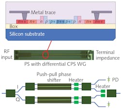
The target design for a high-performance, high-speed modulator must achieve a velocity match between the optical and RF traveling waves, as well as an impedance match between the loaded transmission line (TXL) and terminal impedances. The NeoPhotonics modulator design uses a coplanar strip (CPS) electrode formed by two metal traces. The metal trace width and gap are optimized for the p-n junction as a TXL. Velocity matching is achieved by choosing doping conditions in combination with electrooptic design optimization of the devices.
For accurate simulation of TXL impedance and RF group velocity, an electro-magnetic (EM) model is combined with a p-n junction circuit model (see Fig. 1). Each MZM for I or Q comprises two p-n PS devices to form Mach-Zehnder interferometer (MZI) structures. The p-n junction is made with a lateral structure in a 500-nm-wide rib waveguide and a 90-nm-thick slab, and the heaters are used for MZM phase tuning.Phase-shifter doping
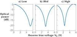
The low doping case is clearly not practical for coherent modulators intended for compact pluggable modules, since either the size would be prohibitive (too long) or the Vπ would be too high.
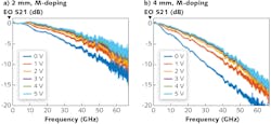
Consequently, mid- and high-doping configurations were explored in the modulator design and fabrication process (see Fig. 3). For mid-doping conditions, the frequency response (EO S21) at different p-n bias voltages for 2- and 4-mm-long phase shifters was analyzed. Essentially, high bias and shorter PS length result in wider electrooptic bandwidth, while low bias and longer PS length result in an increase in modulation efficiency. Test data shows that the 3 dB electrooptic bandwidth of a mid-doped MZM is 22 and 36 GHz using 4- and 2-mm PS lengths, respectively. High doping slightly reduces the bandwidth, but results in higher modulation efficiency.These IQ modulators can be designed for different high-baud-rate applications with tradeoff between doping levels and PS lengths. To evaluate high-baud-rate/high QAM performance, NeoPhotonics fabricated an IQ modulator using a 3.9 mm PS and mid doping with estimated optical loss on the chip of 7.3 dB and a Vπ of 4.1 V. The optical loss of the IQ modulator includes loss from the PS and an assumed 0.5 dB extra loss from the couplers—fiber coupling loss is not included.
Transmission experiments
High-baud-rate modulator testing over telecommunications C-band wavelengths included a NeoPhotonics micro integrated tunable laser assembly (uITLA) with 19 dBm output power and <50 kHz linewidth; a Keysight (Santa Rosa, CA) M8196A arbitrary waveform generator (AWG) with 92 GSa/s and approximately 32 GHz bandwidth; a Keysight N4391A optical multi-channel analyzer (OMA) with 160 GSa/s and around 63 GHz bandwidth; and an optical signal-to-noise ratio (OSNR) loading test station.
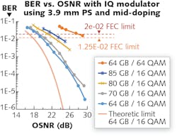
The transmit symbols were generated using pseudo-random data bits of order 15 mapped to Grey-coded QAM symbols. Nyquist shaping with a Root Raise Cosine roll-off factor alpha of 0.2 was used in the test and measured bit error rate (BER) vs. OSNR for the IQ modulator at -2 V p-n bias was recorded (see Fig. 4).Test data at 16 QAM shows that OSNR sensitivity—at the 1.25 e-2 forward error correction (FEC) BER threshold defined in 400ZR—is 19.4 and 23.4 dB, with a 10 dB optical bandwidth of approximately 70 and 90 GHz, for 64 and 85 Gbaud speeds, respectively. Note that for the 64 Gbaud/16 QAM configuration, the corresponding theoretical limit of OSNR sensitivity is 17.6 dB. Test data for 64 Gbaud/64 QAM shows 27.8 dB OSNR sensitivity at the 2.0 e-2 FEC BER threshold, assuming 15% FEC overhead.
Reaching 600G
These experiments show that high-performance, high-speed all-SiPho carrier depletion modulators can be fabricated in a commercial foundry through co-optimizing doping levels and traveling waveguide design by using an accurate electrooptic model for both phase matching and impedance matching in the design. The experimental test data on modulation characterizations under multiple doping conditions agrees well with the simulation data.
By using a 2 mm PS at -2 V p-n bias, the fabricated MZMs achieve 6 dB EO bandwidth of 54 GHz without fast roll-off in the frequency range over 60 GHz with mid-doping conditions. All-silicon IQ modulators operating at 85 Gbaud/16 QAM and 64 Gbaud/64 QAM with high electrooptic bandwidth and >25 dB extinction ratio easily support data transmission of 400 and 600 Gbit/s per wavelength in a compact form factor.
REFERENCES
1. J. Zhou et al., “Silicon photonics carrier depletion modulators capable of 85Gbd 16QAM and 64Gbd 64QAM,” Optical Fiber Conference (OFC) 2019, paper Tu2H.2, San Diego, CA (Mar. 2019).
2. J. Zhou et al., “Model and design of silicon photonic carrier-depletion Mach-Zehnder modulators for 400Gb/s and Beyond PAM & QAM Applications,” Proc. SPIE, 10923, 1092318 (Feb. 2019).
Jianying Zhou is director, design and technology at NeoPhotonics, San Jose, CA; e-mail: [email protected]; www.neophotonics.com.


