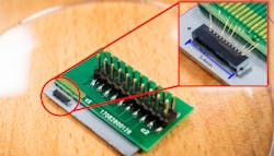
Integrated silicon photonic chip for quantum-key distribution is 3 mm in size
Most leading security standards (algorithm examples of which include Advanced Encryption Standard, or AES, and Rivest-Shamir-Adleman, or RSA, which are used in making online communications such as payments on shopping websites secure) used in secure communication methods do not take advantage of quantum technology. As a result, electronic transmission of personal identification numbers (PINs) or passwords can be intercepted, posing a security risk. To mitigate these risks, researchers at Nanyang Technological University, Singapore (NTU Singapore) have developed a silicon-photonics-based quantum-communication chip that is 1000X smaller than current quantum setups, but offers the same superior (and supposedly uncrackable) security that quantum technology is known for.
Roughly 3 mm in size, the chip, which is compatible with the existing fiber-optic communication infrastructure, uses quantum communication algorithms to provide enhanced security compared to existing standards. It does this by integrating passwords within the information that is being delivered, forming a secure “quantum key.” After the information is received, it is destroyed along with the key, making it an extremely secure form of communication. It is far smaller than current quantum communication setups that can be in some cases as big as a refrigerator, and in others, can take up the space of an entire room. The compact size opens doors for more secure communication technologies that can be deployed in compact devices such as smartphones, tablets, and smart watches. It also lays the foundation for better encryption methods for online transactions and electronic communication. The chip, which operates at a 1550 nm wavelength, includes amplitude and phase modulators that generate a series of quantum coherent states; information is encoded on a 1–10 MHz sideband. The NTU team is now looking to develop a hybrid network of traditional optical communication systems and quantum communication systems. Reference: G. Zhang et al., Nat. Photon. (2019); https://doi.org/10.1038/s41566-019-0504-5.
About the Author
John Wallace
Senior Technical Editor (1998-2022)
John Wallace was with Laser Focus World for nearly 25 years, retiring in late June 2022. He obtained a bachelor's degree in mechanical engineering and physics at Rutgers University and a master's in optical engineering at the University of Rochester. Before becoming an editor, John worked as an engineer at RCA, Exxon, Eastman Kodak, and GCA Corporation.

