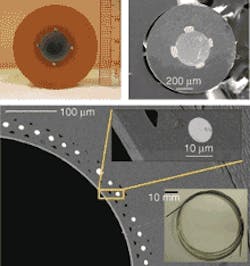
Optoelectronic devices owe their functionality to the combination of conducting, semiconducting, and insulating materials, and are typically manufactured in wafer-based processes and restricted to planar geometries. But a team of researchers including Mehmet Bayindir and other members of the Fink lab at the Massachusetts Institute of Technology (MIT; Cambridge, MA) are changing that norm. Building on previous accomplishments, these researchers are extending the traditional planar geometry of these optoelectronic devices to the cylindrical geometry of drawn optical fibers.1-4 Their metal-insulator-semiconductor optical fibers have led to the creation of two prototype fiber structures: a dual electron-photon transport fiber, and a tunable narrowband fiber photodetector.
The electron-photon transport fiber is composed of a hollow core surrounded by a dielectric mirror formed from eight pairs of alternating layers of arsenic selenium (an amorphous semiconductor), and a high-glass-transition-temperature insulator called polyetherimide (see figure). Adjacent to the omnidirectional mirror is a circular array of 60 tin metal strands with diameters of approximately 8 mm. The entire fiber is surrounded with a polyethersulphone polymer cladding. Optical-transport characteristics of the fiber are determined by the positions of the photonic bandgaps; fibers having outer diameters of 980, 1030, and 1090 µm have fundamental bandgaps centered at 1.62-, 1.75- and 1.85-µm wavelengths, respectively. Initial broadband cutback measurements on an electron-photon fiber with length of 1 m and core size of 800 µm yielded a transmission loss of 4.9 dB/m and a bending loss of 0.9 dB for a 90° bend with a bending radius of 6 cm. By coating both ends of the fiber with a thick layer of gold to electrically connect all the tin wires, a linear current-voltage response is observed. Because of the unique construction of these electron-photon fibers, electrical and optical transmissions are spatially separated and the electrons and photons being transmitted do not interact.
Integrated optoelectronic fibers
While the electron-photon fiber displays the unique attributes of a metal-semiconductor-insulator structure, the researchers see it as a precursor to more-important capabilities. “These structures represent a new way of thinking about optical fibers as integrated optoelectronic devices, with the potential to perform multiple optical, electronic, and optoelectronic functions over long lengths and with fiber cost scales,” says Yoel Fink. One such variation on the fiber for separate electron and photon transmission is a fiber design that uses an optoelectronic interaction. The fiber core in this case is arsenic selenium tellurium tin (a highly photoconductive glass) conta (see figure). Upon external illumination, the conductivity of the semiconductor is changed and is measured through the metal leads terminated at the end of the fiber. This fiber photodetector exhibits a broadband response.
The MIT team then constructed a narrowband detector by surrounding the core with a photonic-bandgap resonant-cavity structure. The photonic bandgap and resonance wavelength are determined by the outer diameter of the fiber. Three different prototype fibers were fabricated with diameters of 870, 890, and 920 µm, corresponding to resonance wavelengths of 1.26, 1.29, and 1.33 µm, respectively. When the fiber is illuminated with light at its resonance wavelength, back-reflection is diminished and the light reaches the photoconductive core, producing measurable photocurrent. These unusual fiber photodetectors could be used to construct a functional optoelectronic fabric that could be woven into a two-dimensional optical-detector array, enabling large-area detection, as only 2N fibers are needed to achieve illumination detection at N2 resolution.
Although these prototype optical fibers were drawn from preforms only a fraction of the size of conventional optical fibers, improvements in the fiber-drawing process will undoubtedly continue. As these processes are refined, longer drawing lengths will be possible, allowing the number of applications for these fibers to grow.
REFERENCES
- Y. Fink et al., Science 282, 1679 (November 1998).
- Hart et al., Science 296, 510 (April 2002).
- Temelkuran et al., Nature 420, 650 (December 2002).
- M. Bayindir et al., Nature 431, 826 (Oct.14, 2004).

Gail Overton | Senior Editor (2004-2020)
Gail has more than 30 years of engineering, marketing, product management, and editorial experience in the photonics and optical communications industry. Before joining the staff at Laser Focus World in 2004, she held many product management and product marketing roles in the fiber-optics industry, most notably at Hughes (El Segundo, CA), GTE Labs (Waltham, MA), Corning (Corning, NY), Photon Kinetics (Beaverton, OR), and Newport Corporation (Irvine, CA). During her marketing career, Gail published articles in WDM Solutions and Sensors magazine and traveled internationally to conduct product and sales training. Gail received her BS degree in physics, with an emphasis in optics, from San Diego State University in San Diego, CA in May 1986.