Minimizing taper improves light gathering
For fiber-coupled charge-coupled-device (CCD) imagers operating over large fields of view, size matters. This is because the amount of light that actually reaches the detector decreases in inverse proportion to the square of the fiber-to-CCD taper ratio. Accordingly, engineers at Fairchild Imaging (Milpitas, CA) have developed what the company claims is the largest commercially available CCD—a 4096 × 4096-pixel sensor with a surface area slightly larger than 6 × 6 cm, making possible a taper-free (1:1) fiberoptic-coupled camera for scientific x-ray imaging.
The device has actually been shipping to an OEM customer for crystallography applications for several years, but has recently become available to end users in other x-ray imaging applications, said Colin Earle, director of advanced camera systems, who described the device at Photonics West 2004 (Jan. 24–29; San Jose, CA). In protein crystallography, a large-area imager is required to capture the full scatter pattern with the required definition.
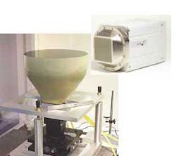
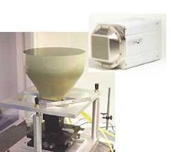
In addition to the 1:1 coupling coupled to a 90-mm fiberoptic plate (inset), the same CCD has also been bonded in a 1.5:1 taper to a 135-mm fiberoptic plate, and a 2.3:1 taper to a 200-mm fiberoptic plate (shown here), which Earle described as the world's largest commercially available taper. Bonding a CCD to fiber is a nontrivial matter in such sizes and applications, partially because the joint undergoes considerable mechanical stress when the camera is cryogenically cooled to -60°C to minimize dark current. The entire optical-cement surface must be kept free of bubbles, cracks, and contaminants, and then cured for a week or two before being assembled into the camera, Earle said.
Fairchild Imaging specializes in large-wafer-scale devices, and a camera with an even larger CCD sensor—9000 × 9000 pixels and 8 × 8 cm in surface area—is currently being used in aerial-reconnaissance applications. The company is not actively marketing that device, but it is available, Earle said.

