Microstructured Fibers: MSEM models holey fiber drawing process
Microstructured, holey, or photonic-crystal fibers used in supercontinuum generation and sensing applications have a complex structure that is difficult to model; prediction of the final performance parameters and required fabrication dimensions and process steps is often an empirical trial-and-error process that takes many months. However, using a variant of the discrete-element method, researchers at the University of Southampton (England) have developed a microstructure-element method (MSEM) that significantly improves upon existing methods to model and accurately predict final fiber dimensions and cross-section distortions for a broad range of microstructured fibers, including those with high air-filling fraction and thin internal membranes.1
A complex case: HC-PBGFs
To demonstrate how the model addresses the simplest (a few holes) to the most complex (hundreds of holes) microstructured optical fibers, the researchers apply the model to one of the most challenging fiber types: a hollow-core photonic-bandgap fiber (HC-PBGF).
Most holey fibers are fabricated in a two-step draw process. A series of stacked capillary tubes is first assembled, heated, and drawn to a desired diameter. Next, a thick outer cladding tube is placed over the initial preform, and the entire structure is drawn into fiber.
Existing modeling techniques use either finite-element methods or the boundary-integral method, but these have only been successful in predicting fiber performance and draw parameters for up to six holes. In fact, the mesh requirements (that scale with the number of struts—the fine membrane structures surrounding the holes of the fibers) would result in an inordinately slow calculation process as the number of holes increased.
In experimental draws of real HC-PBGFs, wherein nodes are separated by highly viscous liquid glass struts, the forces acting upon the various nodes are a function of glass parameters, gas pressures during the draw, and drawing temperatures.
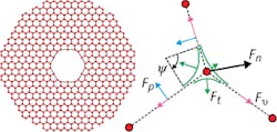
Similarly to how the discrete-element method applies interaction forces to discrete bodies or Lagrangian particles and then evolves the forces over time in a particular fabrication process, the MSEM method considers the nodes (or junctions where the fiber struts meet) as a particle acted upon by fabrication forces during the fiber draw process (see figure). Pressure, viscosity, and surface tension forces acting through the struts on the nodes of the fiber are identified, node positions are adjusted, and the simulation is advanced over time. A 2D axisymmetric model derived from the Navier-Stokes equations, developed in another study, is used to solve the shape of the outer cladding tube; this is used to scale the internal structure as it is drawn down to fiber.
Modeled results
Using MSEM, comparison of final fiber parameters both predicted from the modeled draw parameters and experimentally computed from the final fibers themselves are in excellent agreement; that is, the difference between core ratio of the experiments and the simulations does not exceed 4%.
“One of our objectives at Southampton is to reduce the transmission loss of hollow-core photonic-bandgap fibers for telecom applications,” says Gregory Jasion at the University of Southampton. “Finding the perfect structure, and the procedure to make it, is a necessary part of that. In an experimental draw there is only enough time to try a handful of parameters, but this model is extremely quick, allowing us to explore a huge range of draw parameters and more radical ideas. We can then apply this knowledge to make better fibers.”
REFERENCE
1. G. T. Jasion et al., Opt. Exp. 23, 1, 312–329 (Jan. 12, 2015).

Gail Overton | Senior Editor (2004-2020)
Gail has more than 30 years of engineering, marketing, product management, and editorial experience in the photonics and optical communications industry. Before joining the staff at Laser Focus World in 2004, she held many product management and product marketing roles in the fiber-optics industry, most notably at Hughes (El Segundo, CA), GTE Labs (Waltham, MA), Corning (Corning, NY), Photon Kinetics (Beaverton, OR), and Newport Corporation (Irvine, CA). During her marketing career, Gail published articles in WDM Solutions and Sensors magazine and traveled internationally to conduct product and sales training. Gail received her BS degree in physics, with an emphasis in optics, from San Diego State University in San Diego, CA in May 1986.
