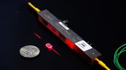
Monolithic integrated lithium niobate modulator operates at CMOS voltages of about a volt
Lithium niobate (LN) modulators are widely used across the optics and photonics industry. Now, researchers from Harvard University's John A. Paulson School of Engineering and Applied Sciences (SEAS; Cambridge, MA) have developed a new method to fabricate and design integrated on-chip LN modulators 100 times smaller and 20 times more efficient than current LN modulators.1
LN modulators are the backbone of modern telecommunications, converting electronic data to optical information in fiber-optic systems. However, conventional LN modulators are bulky, expensive, and power hungry. These modulators require a drive voltage of 3 to 5 V, significantly higher than that provided by typical CMOS circuitry, which provides about 1 V. As a result, separate, power-consuming amplifiers are needed to drive the modulators, severely limiting chip-scale optoelectronic integration.
The Harvard team created monolithically integrated LN modulators with a CMOS-compatible drive voltage that support data rates up to 210 Gbit/s and have an on-chip optical loss of less than 0.5 dB. "This research demonstrates a fundamental technological breakthrough in integrated photonics," says Marko Loncar, the Tiantsai Lin Professor of Electrical Engineering at SEAS and senior author of the paper. "Our platform could lead to large-scale, very fast and ultra-low-loss photonic circuits, enabling a wide range of applications for future quantum and classical photonic communication and computation."
Harvard's Office of Technology Development (OTD) has worked closely with the Loncar Lab on the formation of a startup company, HyperLight, that intends to commercialize a portfolio of foundational intellectual property related to this research. Readying the technology toward the launch of HyperLight has been aided by funding from OTD’s Physical Sciences & Engineering Accelerator, which provides translational funding for research projects that show potential for significant commercial impact.
Lithium niobate is considered by many in the field to be difficult to work with on small scales, an obstacle that has so far ruled out practical integrated, on-chip applications. In previous research, Loncar and his team demonstrated a technique to fabricate high-performance LN microstructures using standard plasma etching to physically sculpt microresonators in thin lithium niobate films.
Source: https://www.seas.harvard.edu/news/2018/09/small-modulator-for-big-data
REFERENCE:
1. Cheng Wang et al., Nature (2018); https://doi.org/10.1038/s41586-018-0551-y.

John Wallace | Senior Technical Editor (1998-2022)
John Wallace was with Laser Focus World for nearly 25 years, retiring in late June 2022. He obtained a bachelor's degree in mechanical engineering and physics at Rutgers University and a master's in optical engineering at the University of Rochester. Before becoming an editor, John worked as an engineer at RCA, Exxon, Eastman Kodak, and GCA Corporation.
