Laser Focus World’s top 20 photonics technology picks for 2020
The technology covered by Laser Focus World can perhaps be loosely categorized as “anything having to do with photons”—although with certain prerequisites, of course, including usefulness, originality, and a reasonably high technical level. As a result, we are not the sort of publication that focuses on a single market; rather, our coverage enthusiastically spans the gamut of human expertise (well, as long as photons are involved).
Thus, picking a top 20 list of this past year’s technical achievements in photonics presents a conundrum, as both the types of technology and the markets we cover can be easily divided and subdivided so that each list contains more than 20 items. The resulting picks are therefore just a sampling of the technologies and markets we cover. The picks below are loosely sorted into arbitrary groups, with no ranking from better or worse; due to the skills and inventiveness of the engineers, technicians, and scientists who worked in the photonics arena in 2020, every item here is the cream of the crop and should be at the top of the list (note: you will find a number of deep learning and AI-related applications here, mostly related to imaging).
Advances in fiber optics
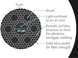
1. Hollow-core optical fiber channels light through an air-filled core using a phenomenon such as a photonic bandgap or antiresonance. Through years of research, optical loss in this type of fiber has been greatly reduced. One of the great advantages of this fiber is a higher data-transmission speed, as light travels substantially faster through air than through glass. This year, OFS (Somerset, NJ) commercially introduced a photonic bandgap hollow-core fiber aimed at a market that especially values high-speed transmission—high-frequency traders (see Fig. 1). The OFS fiber can replace microwave transmission in the “last-mile” connection between the microwave tower and the datacenter; its speed advantage over glass fiber shaves valuable milliseconds from the time between trading transactions, increasing traders’ profits. (See “Hollow-core fiber gives high-frequency traders an edge,” October 2020 issue; https://bit.ly/2020TechRev1.)2. High-power laser light can be easily ducted to its point of application via optical fiber. However, existing solid-core chalcogenide glass fibers used in mid-infrared (mid-IR) applications such as surgery and some types of materials processing absorb enough light that they can overheat, even resulting in damage. A mid-IR version of antiresonant hollow-core fiber developed at the Optoelectronics Research Centre, University of Southampton (England) and the Center of Materials and Nanotechnologies, University of Pardubice (Czech Republic) solves this problem; the outer surface of the fiber is coated with fluorinated ethylene propylene (FEP) polymer to increase durability and protect the fiber from moisture. The tellurite-glass fiber material has high thermal stability and can be synthesized in an ambient air environment. The fiber is close to single-mode in operation. (See “Tellurite hollow-core antiresonant fiber for mid-IR is quite bendable,” June 2020 issue; https://bit.ly/2020TechRev2.)
3. In the world of ultrafast-laser materials processing, pico- and femtosecond fiber lasers are now making their mark. In these lasers, properties of the active fiber itself are the limit to higher pulse energies. Traditionally, fiber diameter has been increased to enable higher pulse energies, but the beam quality of these large effective mode area (LMA) fibers is highly sensitive to any bending of the fiber. Now, tapered double-clad fiber (T-DCF) amplifiers offer the prospect of high power with excellent beam properties. Developed in the European PULSE project, which includes Tampere University and Ampliconyx Oy (both in Tampere, Finland), T-DCF is a double-clad optical fiber formed using a fiber-drawing process that forms a taper along the length of the fiber. Both the core and cladding are tapered; the result of the changing fiber parameters is a chain of fiber amplifiers with ever-growing core diameter, combining features of conventional small-diameter, double-clad single-mode fibers with those of much larger-diameter, double-clad multimode fibers used for high-power amplification. (See “Tapered double-clad fiber: The future of ultrafast high-power laser processing,” May 2020 issue; https://bit.ly/2020TechRev3.)
Instruments increase their observation capabilities
4. Superresolution optical-fluctuation imaging (SOFI), developed by researchers at the Laboratory of Biomedical Optics at the École Polytechnique Fédérale de Lausanne (EPFL; Lausanne, Switzerland), is a new microscopy technique for biology that, unlike other multicolor fluorescence techniques, encourages crosstalk between different spectral channels of the microscope; this allows a statistical analysis to be done that creates additional "virtual" spectral channels. The software algorithm statistically analyzes higher-order spatiotemporal statistics of a time series of blinking fluorophores, and as a result does not require the isolation of individual fluorophores′ emissions. The seemingly complex technique actually simplifies fluorophore selection and experiments. (See “Superresolution optical-fluctuation imaging microscopy is multicolor,” July 2020 issue; https://bit.ly/2020TechRev4.)
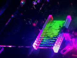
5. Light-sheet fluorescence microscopy (LSFM) illuminates a plane of a sample, allowing a 2D section of the sample to be imaged. An improvement to LSFM has been made by a group at the University of Hong Kong; called coded light-sheet array microscopy (CLAM), the technique allows capturing of data from multiple light sheets simultaneously, negating the need for time-consuming scanning of a single light sheet through the sample to get a 3D image. Light from a single source is bounced between two mirrors to create multiple sources, with path-length differences creating incoherence between the sources (see Fig. 2). A unique code is imposed on each source via a rotating reticle that impresses a different modulation frequency on each beamlet; a cylindrical lens then creates the set of light sheets. Up to 40 simultaneous light sheets were demonstrated. (See “Coded light sheets improve fluorescence volume imaging,” June 2020 issue; https://bit.ly/2020TechRev5.)6. White-light interferometry is a proven method for ultraprecise 3D surface metrology; however, the information it provides can be augmented. KLA Instruments (Milpitas, CA) has developed an interferometric 3D optical profiler that combines color images of the area being mapped with the data from the interferometer using sensor-fusion techniques, providing a precise color 3D surface profile map. In addition, data from other sensors can be included to add even more types of data. White-light interferometry (WLI), phase-shift interferometry (PSI), True Color imaging (KLA’s brand name), and stitching (combining numerous adjacent image fields to create a larger field) into one optical profiler to characterize flexible electronic devices, materials, and fabrication processes. A composite WLI + PSI technique enables greater than 10X higher vertical resolution than WLI and is useful for characterizing smoother surfaces, while the addition of color augments capabilities; for example, in inkjet-printing of conductor layers, overlapping regions exhibit color variations readily visible in the True Color images. (See “3D optical interferometry with True Color visualization advances understanding of flexible electronics,” September 2020 issue; https://bit.ly/2020TechRev6.)
7. Single-molecule microscopy can potentially examine interactions between individual molecules within intact cells; however, interactions between these molecules occur at a scale at least 4X smaller than what can be resolved by existing single-molecule microscopes. “The reason why the localization precision of single-molecule microscopes is around 20 to 30 nm normally is because the microscope actually moves while we’re detecting that signal,” says Katharina Gaus, head of the University of New South Wales (UNSW; Sydney, Australia) Medicine’s EMBL Australia Node in Single Molecule Science. The UNSW team greatly improved stabilization to better than 1 nm and localization precision to about 1 nm by inserting a feedback loop between the sample and stage position and an autonomous optical feedback loop in the emission path, and by characterizing and chromatically correcting of the microscope's EMCCD camera. The feedback system designed by the UNSW team is compatible with existing microscopes. (See “Self-aligning microscope overcomes limits of superresolution microscopy,” Laser Focus World online [April 23, 2020]; https://bit.ly/2020TechRev7.)
8. Digital optical holograms are used in quantitative phase microscopy (QPM) systems for long-term live-cell imaging; here, illuminating light at low levels is used to capture cells at subcellular resolutions as they carry out their activities in their natural environment. However, the low light levels tend to lead to low-quality holograms that appear grainy due to the fundamental noise limit, which is shot noise. A team at Australian National University (ANU; Canberra, Australia) has circumvented this problem by using a neural network called Holo-UNet, trained via thousands of learning cycles, to denoise the holograms. Holo-UNet learns the changes along parallel intensity fringes in the area of a phase object in the field of view and, after training, removes superfluous intensity changes and shot-noise-related intensity changes, improving fringe visibility. Using very little light (almost pitch-black at submillisecond imaging speeds), the setup can still restore a hologram to close-to-perfect condition. (See “Neural network greatly improves shot-noise-limited microscopy holograms,” October 2020 issue; https://bit.ly/2020TechRev8.)
9. Researchers at the Medical University of Vienna (Austria) are using deep learning in the form of convolutional neural networks (CNNs) to segment ophthalmic OCT images in order to recognize the eye’s tear meniscus, which is the layer of liquid present as the eyelid traverses the surface of the eye. Patients suffering from dry-eye disease have abnormal meniscus geometries, quantifiable with measures such as tear meniscus volume, height, or radius of curvature. Such measurements need the tear meniscus to be separated from other regions in an image, which a CNN can potentially do more reliably than a human. Two new approaches, a one-phase neural network that segments the tear meniscus from a large OCT image and a two-phase neural network that first selects a region of interest and then segments the tear meniscus from that smaller region, are both as accurate as standard image processing, and are significantly faster. (See “Deep learning for OCT image analysis,” May 2020 issue; https://bit.ly/2020TechRev9.)
Photonic devices for quantum and other uses
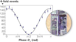
10. The first integrated photon source with the potential to enable large-scale CMOS-process-fabricated quantum photonics has been created by a team of physicists at the University of Bristol (England). The source is based on intermodal spontaneous four-wave mixing (SWFM), in which multiple modes of light propagating through a silicon waveguide are nonlinearly interfered, creating ideal conditions for generating single photons. In contrast to standard SWFM, intermodal SWFM does not produce photons with a strong spectral anticorrelation (the opposite of what is needed in quantum optics circuits). The team benchmarked the use of such sources for photonic quantum computing in a so-called heralded Hong-Ou-Mandel experiment, a building block of optical quantum information processing, and obtained the highest-quality on-chip photonic quantum interference ever observed of 96% visibility (see Fig. 3). The silicon-photonic device was fabricated via CMOS-compatible processes in a commercial foundry; as a result, thousands of sources could be easily integrated on a single device. The researchers plan to integrate tens to hundreds of the quantum sources on a single chip. (See “Silicon-photonic photon source is near-ideal for quantum-optical technologies,” July 2020 issue; https://bit.ly/2020TechRev10.)11. True random-number generators are essential for cryptographic data communications. While so-called pseudorandom numbers can be generated by software algorithms, cryptography built around such numbers can be deciphered with enough time because of the nonrandom basis of the number generation. In contrast, truly random numbers can be generated only by a setup based on a truly random physical process. A new photonics-hardware-based random-bit generator has now been developed by a world-spanning group of researchers; being chip-based, the device is scalable, robust, small, and energy-efficient. The new device is ultrafast—on the order of 100 Tbit/s—which is two orders of magnitude faster than previous physical random-bit generators. The simple device consists of a single gallium arsenide/gallium aluminum arsenide (GaAs/AlGaAs) laser diode with a configuration allowing many spatiotemporally interfering lasing modes, resulting in spontaneous emission noise, and two arrays of photodetectors to sense the noise. (See “Hourglass-shaped laser-diode cavity forms a parallel ultrafast random-bit generator,” May 2020 issue; https://bit.ly/2020TechRev11.)
12. The first megapixel photon-counting camera based on new-generation image-sensor technology that uses single-photon avalanche diodes (SPADs) has been developed by researchers at the Advanced Quantum Architecture Laboratory (AQUALab) at École Polytechnique Fédérale de Lausanne (EPFL; Lausanne, Switzerland). With a pitch of 9.4 µm, the camera's pixels are some of the smallest SPAD pixels ever devised, and have a per-pixel power consumption of less than 1 μW while maintaining speed and timing precision. The new camera acquires images at rates up to 24,000 frames per second (fps). Sophisticated integrated-circuit-design techniques were applied to create an extremely uniform distribution of fast electrical signals over the large-scale pixel array; the shutter speeds varied by only 3% over the megapixel array. The camera has projected uses in virtual reality and lidar. (See “Photon-counting camera has megapixel SPAD array for single-photon TOF and other imaging,” Laser Focus World online [April 16, 2020]; https://bit.ly/2020TechRev12.)
13. The midwave- to longwave-infrared (MWIR to LWIR) spectral regions are important for applications that include environmental monitoring, gas sensing, thermal imaging, food and pharmaceutical quality control, and others; however, existing MWIR and LWIR detectors are typically complex and expensive. While lead sulfide (PbS) colloidal quantum dots (CQDs) have emerged as a cost-competitive and high-performance photodetector technology compatible with CMOS technology, they have previously demonstrated success only to the shortwave-infrared (SWIR) region. Now, researchers at ICFO, The Institute of Photonic Sciences (Barcelona, Spain) have created a CQD photodetector that is capable of detecting light in the LWIR, using PbS CQDs that, for the first time, are made with mercury-free material. The devices have responsivities on the order of 10-4 A/W at 80 K in the 5–9 µm range. The spectral coverage of the detectors can be tuned by changing the size of the dots—the larger the CQDs, the farther the absorption in the IR. (See “Quantum-dot photodetectors can now detect longwave infrared light,” Laser Focus World online [January 17, 2020]; https://bit.ly/2020TechRev13.)
Optics and optical materials
14. Thin-film deposition processes, in particular ion-beam sputtering (IBS), for multilayer optical coatings can cause stress in the coatings, which in turn can stress the underlying optic, possibly warping it. Now, researchers at Colorado State University (Fort Collins, CO) have developed an improved IBS process that can deposit high-optical-quality silicon dioxide (SiO2) thin films with residual stress reduced from 490 MPa to 48 MPa using high-energy O2-assist ion bombardment during thin-film deposition. The results are intended to improve the fabrication of high-reflectance tantalum pentoxide/silicon dioxide (Ta2O5/SiO2) multilayer stacks, in particular for thin mirrors used for adaptive-optical (AO) wavefront correction. SiO2 films from an oxide target were deposited with 48 MPa residual stress and an optical absorption of less than 20 parts per million (ppm) at a 1064 nm wavelength, with less than 9 ppm sometimes achievable. (See “Ion-beam-deposited silicon-dioxide optical thin films have 10X less residual stress,” Laser Focus World online [March 24, 2020]; https://bit.ly/2020TechRev14.)
15. Infrared (IR) thermal imaging is heavily used by the military, surveillance, and security communities to spot and characterize bad behavior. Spoofing thermal imaging is not easy, but researchers at the University of California, Berkeley have created a way to do this by embedding visual “decoys” into surfaces of objects in a way that can fool IR cameras and systems into thinking that the decoy surfaces are at a different temperature than they are. In addition, when the temperature of the object changes, the apparent temperature of the decoy surfaces doesn't. The surfaces contain special structures made from thin films of tungsten-doped vanadium dioxide, in which the level of tungsten doping varies from front to back in the coating. Vanadium dioxide is a substance that at certain temperatures can phase-shift from an insulator, which suppresses electric conductivity, to a metal, which conducts electricity. Doping the structure with various levels of tungsten shifts the phase-shift temperature, and thus the decoy temperature, to anywhere between 15° and 70°C. In addition, the emissivity of the decoy surface is designed to vary with temperature as the inverse of T4 (temperature to the fourth power), which exactly counteracts the T4 dependence of blackbody radiation. (See “Graded metal/insulator coating can create false constant-temperature infrared images,” Laser Focus World online [July 27, 2020]; https://bit.ly/2020TechRev15.)
16. In datacenters, computer backplanes connect printed-circuit boards together to form a computer bus. Here, changing the backplane communication method from electrical to optical can greatly raise data transmission rates, helping to enable high-performance computers (HPCs). A group at the Huazhong University of Science and Technology (Wuhan, China) has developed a high-speed, large-capacity, compact optical backplane based on optical polymer waveguides on a glass substrate that uses vertical-cavity surface-emitting lasers (VCSELs) emitting at 850 nm for data transmission. The backplane network reaches 15 Gbyte/s error-free data transmission via eight parallel channels; in the optical backplane, the 10 Gbit/s in a channel is processed error-free by field-programmable gate-array chips. An experimental platform was built to test the backplane: a pseudorandom bit-sequence signal was modulated via an optical module transceiver; the optical signal was transmitted through a coupler and four ports of the 1 × 8 parallel polymer waveguide array, then transmitted via another coupler to a second transceiver that did an optical-to-electrical conversion. Finally, bit-error-rate correction was done. For all four channels, the bit-error count was zero. (See “Optical polymer waveguide backplane for high-performance computers has zero bit-error count,” October 2020 issue; https://bit.ly/2020TechRev16.)
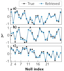
17. For some types of imaging systems, such as microscopes where objects may be transparent but affect phase, the detection or retrieval of phase information could help improve the imaging process. Phase retrieval, which is the computational recovery of hidden phase information from intensity information, exists but in its conventional forms is slow, requiring intensive computation to retrieve any useful amount of phase information. Scientists at Stanford University (Palo Alto, CA) have developed a phase-retrieval technique (see Fig. 4) based on deep residual neural networks (NNs) that quickly and accurately extracts the hidden phase for general point-spread functions (PSFs). The NN processes the information and outputs Zernike coefficients of orders 1 through 6 (corresponding to so-called Noll indices of 2 through 28). A large number of training PSFs were required: 200,000 was not enough, and the researchers finally settled on an amount of 2,000,000 PSFs. The approach can potentially be expanded to do phase retrieval of non-Zernike-like phase information, and could also be helpful in the design of phase masks. (See “Deep neural network accurately retrieves phase information from 3D point-spread functions,” January 2020 issue; https://bit.ly/2020TechRev17.)Other top picks
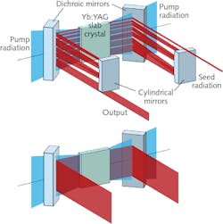
18. While the earlier-mentioned pico- and femtosecond fiber lasers have many remarkable qualities, for the highest-average-power ultrafast light, one must turn to bulk solid-state lasers. Researchers at the Fraunhofer Cluster of Excellence Advanced Photon Sources (CAPS; several locations in Germany) aim to not only overcome ultrafast laser power limitations, but also develop technologies along the process chain from pulse generation to process technology, and real-world applications. Using the InnoSlab technique (a rectangular crystal between two heat sinks that is longitudinally pumped by collimated laser diodes), an ultrafast amplifier has been built that emits compressed pulses of a little more than 1 mJ energy at 500 kHz, resulting in an average power of 530 W (see Fig. 5). Using a gas-filled Herriott-type cell, the researchers have demonstrated pulse-duration reductions from 590 to 30 fs with less than 5% of the energy lost. The CAPS project is aiming at ultrafast-laser average output powers of 10 to 20 kW. (See “Ultrashort-pulsed laser sources with kilowatt power for industrial applications,” January 2020 issue; https://bit.ly/2020TechRev18.)19. Printing of semiconductor components is a relatively young process, but the optoelectronics industry is already making large investments in the production of printed OLED displays and flexible solar cells; scientists at the Karlsruhe Institute of Technology (KIT; Germany) have now created printable organic photodiode detectors that can see colors, useful for visible light communication (VLC) and other applications. The photodetection molecules consist of nonfullerene acceptors (NFAs), which are embedded in a transparent polyindenoflurorene-8-triarylamine (PIF) polymer matrix. Different NFAs produce different color-absorbing bands—for example, in the red and in the blue-green. The researchers inkjet-printed a dual-color VLC system as a demonstration of the color-selective organic photodiodes; they say that their very simple setup could go as high as 3.5 Mbit/s transmission. (See “Simple inkjet-printed color-selective organic photodiodes require no optical filters,” March 2020 issue; https://bit.ly/2020TechRev19.)
20. Almost two million people worldwide suffer from retinitis pigmentosa (RP), an incurable degenerative disease that damages photoreceptors in the retina and eventually leads to blindness. LambdaVision (Farmington, CT) is developing a structured bacteriorhodopsin-based implant with potential to restore high-quality vision to patients with irrecoverable damage to their photoreceptors. In the device, a single-molecule-thick bacteriorhodopsin layer is covered with a polycation polymer; several additional identical bacteriorhodopsin/polycation layers are deposited to form the complete implant. Inherent electrostatic forces align and stabilize the molecules, and the resulting oriented multilayered architecture has the optical density required to absorb light and generate a sufficient ion gradient for retinal stimulation. In addition to mimicking the electro-optical properties of rods or cones, the ambient environment in the eye provides the protons necessary to accommodate the cyclic bacteriorhodopsin proton-pumping mechanism. No external power is necessary. (See “Self-powered artificial retina uses light-activated protein to enable ‘meaningful sight,’” August 2020 issue; https://bit.ly/2020TechRev20.)
About the Author
John Wallace
Senior Technical Editor (1998-2022)
John Wallace was with Laser Focus World for nearly 25 years, retiring in late June 2022. He obtained a bachelor's degree in mechanical engineering and physics at Rutgers University and a master's in optical engineering at the University of Rochester. Before becoming an editor, John worked as an engineer at RCA, Exxon, Eastman Kodak, and GCA Corporation.

