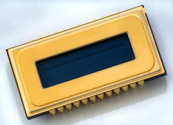
The S11500-1007 back-thinned CCD for Raman spectroscopy from Hamamatsu Photonics (Bridgewater, NJ) offers a spectral response range from 200 to 1100 nm, and features 40% quantum efficiency at 1000 nm. Proprietary laser processing technology forms a MEMS structure on the back side of the CCD, making it sensitive in the NIR region for detecting long-wavelength Raman emissions. Binning allows linear image sensor operation.
-----
PRESS RELEASE
Hamamatsu introduces a new IR-enhanced CCD image sensor for Raman spectroscopy
Hamamatsu Corporation has introduced the S11500-1007 back-thinned CCD for Raman spectroscopy. This CCD has a wide spectral response range from 200 nm to 1100 nm, and features 40% quantum efficiency at 1000 nm. Its enhanced sensitivity in the NIR region, which is particularly beneficial for detecting long-wavelength Raman emissions, is made possible by applying Hamamatsu's unique laser processing technology to form a MEMS structure on the back side of the CCD.
The S11500-1007 has 1024 (H) x 122 (V) pixels with a pixel size of 24 x 24 µm. With binning, the CCD can be operated as a linear image sensor. The binning operation ensures even higher signal-to-noise ratio and faster signal processing speed compared to methods that use an external circuit to add signals digitally. The S11500-1007 comes in a 24-pin ceramic DIP package with a quartz glass window. It can be used in conjunction with Hamamatsu's C7040 multichannel detector head (sold separately).
-----
Subscribe now to Laser Focus World magazine; it's free!
