By Hamamatsu Corporation
Through various MEMS (micro-electro-mechanical systems) processes, we fabricate microstructures such as electrostatic actuators, membranes, beam splitters, and mirrors on silicon. Combining these microstructures with photodetectors adds more, or new, functions to the photodetectors and reduces their size.
MEMS devices have many benefits, such as higher performance, sophisticated functions within a compact package, robustness, and cost-effectiveness. To learn more about our MEMS-based micro-spectrometers and MEMS-FPI sensors, see the sections below.
Micro-spectrometers
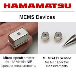
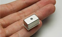
The MEMS processes we use to fabricate components allow our micro-spectrometers to be about the size of a fingertip—a fraction of traditional modular spectrometers. The micro-spectrometer comes in a hermetically sealed package, which makes it usable in adverse conditions (e.g., high humidity) that traditional spectrometers do not tolerate well.
A micro-spectrometer's compact package makes it easy to integrate into equipment and instruments such as printers, handheld color monitors, and environmental monitors. The micro-spectrometer can also be integrated into a small circuit module, and the module can be connected to smart phones or tablets to perform handheld spectral measurements.
Structure and operating principle
A micro-spectrometer consists of a grating chip and a CMOS image sensor chip that face each other with an air gap between them. Both chips are enclosed within a small hermetic package. To perform spectral measurements with the micro-spectrometer, light is guided into the entrance slit. The light is then diffracted by the reflective diffraction grating, and the separated wavelengths impinge on the CMOS linear image sensor's pixel array. Each pixel on the sensor receives a particular wavelength of light and outputs an electrical signal proportional to the light's intensity.
The MEMS fabrication techniques used to fabricate these chips include nanoimprinting to form the reflective diffraction grating and deep etching to form an entrance slit on the CMOS sensor chip. Etching the slit in silicon—instead of using a traditional metal slit—reduces the size of the spectrometer.
Products
- C12880MA micro-spectrometer: 340-850 nm spectral response range
- C12666MA micro-spectrometer: 340-780 nm spectral response range
To learn more about micro-spectrometers, go to our website: www.hamamatsu.com
MEMS-FPI sensor for NIR spectral measurement
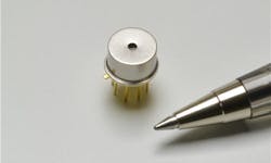
The MEMS-FPI spectrum sensor features an ultra-compact Fabry-Perot interferometer (FPI) and an NIR-sensitive InGaAs PIN photodiode. The Fabry-Perot interferometer acts as a tunable filter and is drastically reduced in size using MEMS technology.
The MEMS-FPI spectrum sensor can be used for in situ spectrum analysis of a variety of substances including gases (environmental measurements), food and beverages, agricultural products, and petrochemical products.
Structure and operating principle
The MEMS-FPI spectrum sensor consists of a MEMS-FPI tunable filter, an InGaAs PIN photodiode, and wiring board. The MEMS-FPI tunable filter is a miniature Fabry-Perot interferometer that consists of a movable upper mirror and fixed lower mirror with an air gap between them. The upper and lower mirrors act as wavelength-tunable parallel plates: the width of the air gap controls the resonant frequency of the cavity and allows certain wavelengths to pass. The upper mirror's movement is controlled through an applied voltage. Applying different voltages results in transmitting a spectrum of wavelengths to be detected by the InGaAs PIN photodiode.
Products
- C13272-01 MEMS-FPI: 1550-1850 nm spectral response range
- C13272-02 MEMS-FPI: 1550-1850 nm spectral response range, with built-in bandpass filter
To learn more about MEMS-FPI sensors, go to our website: www.hamamatsu.com


