ANDREAS HERMERSCHMIDT AND SVEN KRÜGER
Diffractive optical elements can be used to generate complex light patterns with precisely defined dimensions in a specified plane. Examples include viewfinder patterns, arrangements of multiple lines or circles that can be used for three-dimensional (3-D) surface measurements, and patterns that represent rulers or scales. The diffractive elements that produce these complex light patterns must be designed and fabricated in a sophisticated way.
Diffraction theory
When a laser beam is transmitted through a diffractive optical element (DOE), it can be transformed into an almost arbitrary light pattern in the observation plane. Diffraction theory, which is the key to the theoretical treatment of this matter, can be used to calculate how a certain light wave of finite aperture size will be altered during propagation.
Diffraction computations are based on the electromagnetic-field representation of the light field, not only on its intensity distribution. In the easiest case—referred to as Fraunhofer approximation—the diffraction pattern can be computed simply by a Fourier transformation. The underlying assumption that the light field is coherent and monochromatic is fulfilled in sufficiently good approximation as long as laser sources are modeled. Because only the light-pattern intensity distribution is relevant to the application, the phase of the light field is an important degree of freedom in the numerical computations for the DOE design.
Designing a DOE
A laser module often has an adjustable lens system that creates a focused spot on a screen. If a diffractive element is placed behind the lens of the module, many spots that can form a complex light pattern are observed. The design of the diffractive microstructure requires the simulation of an inverted light propagation from the plane in which the pattern is to be created back to the plane of the DOE. Moreover, it is necessary to describe the interaction between the incident light field and the microstructure properly, which is far from trivial especially if the smallest feature dimensions (referred to as “critical dimension,” or CD) of the surface are as small as the wavelength (λ) of the illuminating light, or even smaller.
For coarse structures with a CD greater than 5λ and a sufficiently small depth, a thin element approximation (TEA) can be applied and the optical element can be described by a complex-valued transmission function that accounts for losses (amplitude effects) and optical delays created by the surface relief (phase effects). This transmission function needs to be determined during the optical-design procedure.
Most diffractive elements have a spatially periodic transmission function that leads to clearly defined spot positions in a given plane of interest, because the constructively interfering waves have diffraction angles θ (in x and y) that satisfy the well-known grating equation mλ = gx,ysin θ, where m is the diffraction order number and gx,y are the x and y (spatial) dimensions of a single period of a periodic diffractive structure.
All possible diffraction angles can be derived from these equations for perpendicular incidence of a plane wave with wavelength λ. For small angles the diffraction orders will appear as an equidistant array of spots in the plane of observation, provided a convergence of the illuminating light wave to that plane. This convergence can be obtained from a focusing lens that needs to be placed at a distance to the plane that equals its focal length. For systems like laser modules, it is most convenient to place the diffractive element between the lens and the plane of observation, which can be changed by adjusting the focal length of the lens or lens system. In this case, the size of the diffraction pattern changes proportional to the distance between the DOE and observation plane, but the shape of the pattern remains unchanged.
The design of the transmission function only influences how much of the incident light is diffracted into which diffraction order, but the propagation direction of the orders is solely affected by the mere geometrical size of its spatial periodicity. The design of the optical element includes two basic steps. First, gx and gy must be selected to determine which diffraction orders of the DOE should be produced by an ideal element with a particular relative power. Second, we use an iterative Fourier-transform algorithm (IFTA) that permits the determination of a transmission function that produces the desired diffraction orders with the correct relative strength.
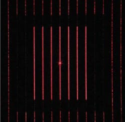
As an example, a DOE can be fabricated that produces M lines consisting of N closely spaced adjacent spots. The angles between spots in the same line are usually much smaller than the angle between the individual lines, so that the condition gx << gy can be easily derived. Using this approach, the DOE does not diffract light into the spaces between the lines, because no diffraction orders are traveling into the corresponding directions. For small diffraction angles, this design approach is very successful (see Fig. 1). However, for larger diffraction angles the lines suffer from geometrical distortions due to small-angle approximations in the diffraction equations.
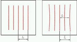
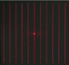
One distortion effect is that the line centers are no longer equidistant. But what is more disturbing for many applications is that the lines appear to be bent (see Fig. 2). If a multiline pattern with a designated area is to be created, this cushion-like geometric distortion leads to an increased area size. For example, if a pattern with an area of 200 × 200 mm needs to be created at a distance of 500 mm from the DOE, the geometric distortion will define an area of 204 × 204 mm, which is not tolerable for some applications.A solution to this problem is the application of a different criterion for the selection of the desired diffraction orders of the grating. A line is constructed from all diffracted waves that produce a spot in the observation plane that is closer to the ideal line position than some width parameter w. For simplicity, if we assume g = gx = gy, the lines are then obtained from a visual anti-aliasing effect created by overlapping spots and it is possible to produce straight lines in the target plane in this way (see Fig. 3). Such DOE elements will usually need to have larger areas gx × gy to provide a sufficiently fine grid of possible spot positions in the target plane. When using such elements in laser modules, for example, the beam diameter should not be too small compared to this area. For laser diodes this requirement is usually not critical with commonly used collimation optics, but diode-pumped solid-state (DPSS) laser modules emitting at 532 nm might have too small a beam diameter and require additional optical elements for beam expansion. The approach used here also requires sufficient suppression of diffraction orders that would propagate into the space between the lines.
DOE fabrication
The fabrication of DOEs requires high-resolution lithographic techniques. For “binary elements” with only two phase levels, the easiest type to fabricate, a chromium amplitude mask is created by a direct-writing process using an electron beam. The substrate of such a mask can be fused silica, which permits the conversion of the amplitude element into a phase element through reactive-ion etching. The areas of the fused-silica wafer that are not protected by the chromium layer are affected by the etching process so that a relief surface profile is created. After removal of the chromium layer, a DOE is obtained.
Diffractive optical elements made from fused silica have a high damage threshold, making them suitable for high-power laser applications. Moreover, they can be used as preforms for the generation of a replication tool. There are several possible replication technologies for diffractive optical microstructures, such as ultraviolet (UV) curing of acrylate materials on various substrates, hot embossing of polymer materials, or injection molding. For applications that require constant diffraction angles and pattern sizes over a wide temperature range, UV curing of polymer materials on glass substrates is an attractive solution that offers lower initial costs compared to injection molding. However, for high-volume applications, the price per piece that can be offered based on injection molding processes is significantly lower so that higher initial costs can be justified, if the thermal expansion of the material and the corresponding variation of the diffraction angles can be tolerated.
Multilevel diffractive elements require a significantly greater effort, especially during the fabrication of the master element. It is possible to use multimask or direct-write approaches to fabricate multilevel structures in photoresist, which can then be transferred into the underlying substrate by reactive-ion etching. The replication of the structures in principle uses the same technologies as for binary elements with only two levels.
Diffractive optical elements can be used to generate a wide range of light patterns with precisely specified dimensions in a particular plane of observation. Different approaches in the design of the optical transmission function of such elements enable optimization with respect to parameters like signal-to-noise ratio or flexibility of spot positions. The fabrication technologies in the mastering and replication steps can be chosen in a way that allows the fulfillment of the specifications at the lowest possible cost for a given production volume.
Andreas Hermerchmidt is a research and development engineer, and Sven Krüger is CTO for HoloEye Photonics, Albert-Einstein-Str. 14, D-12489 Berlin, Germany; e-mail: [email protected].


