JARED WAHLSTRAND, THOMAS DEKORSY, GREGOR KLATT, and STEVEN CUNDIFF
The terahertz (1 THz = 1012 Hz) frequency range lies between microwaves and the infrared. Many vibrational molecular excitations are detectable in the terahertz range, making it a useful band for chemical detection, with applications in industrial settings and in homeland security. Coupling a source of short pulses of terahertz radiation with electro-optic sampling enables terahertz time-domain spectroscopy, allowing for simultaneous ultrafast measurements of the real and imaginary parts of the response of a medium in the far infrared.1,2 With terahertz-emitting modelocked femtosecond lasers still not available, the easiest way to generate terahertz pulses involves using a modelocked laser at optical wavelengths. Note that a short terahertz pulse, which has a duration of less than 1 picosecond, corresponds to an electric field that tracks the intensity envelope of a subpicosecond optical pulse.
While a lot of effort is now being directed at developing high- peak-power terahertz sources—which can be used to study nonlinear optics at terahertz frequencies—for linear spectroscopy the average power, not the peak power, is important. High-repetition-rate (50–1000 MHz) femtosecond sources are simpler, cheaper, and less noisy than sources based on amplified laser systems. By using two synchronized pulsed lasers, one of which generates terahertz pulses while the other detects the terahertz electric field, one can even create a terahertz spectroscopy system without any mechanical moving parts.3 Here we discuss some recent developments in high-repetition-rate terahertz sources based on semiconductors. Note that it is not possible to cover here all the developments that have taken place in recent years in this rapidly growing field, but we discuss a few examples.
Photoconductive emission
There are essentially two mechanisms for producing terahertz radiation from optical pulses. The simplest is optical rectification. In a transparent medium without inversion symmetry, a strong optical pulse induces a dipolar charge distribution that moves with the pulse and emits terahertz radiation. Materials such as the wide-bandgap semiconductor zinc telluride (ZnTe) or organic nonlinear crystals such as DAST are typically used. Optical rectification has the advantage of simplicity: All one need do is focus light from a modelocked laser into a crystal. A disadvantage is the limited bandwidth achievable because of the absorption in the crystal. Additionally, optical rectification requires phase matching: To efficiently produce a short terahertz pulse, the group velocity of the optical pulse needs to match the phase velocity of the terahertz wave.
The second generation mechanism, which we focus on here, is photoconductive emission.4 In this case the terahertz pulse is emitted by accelerating photoexcited carriers generated by an ultrafast pulse impinging on a semiconductor—usually gallium arsenide (GaAs) for a Ti:sapphire laser or indium gallium arsenide (InGaAs) for a fiber laser. An electric field present in the semiconductor results in a current surge that emits a burst of terahertz radiation. Strong electric fields are naturally present at the surface of doped semiconductors, but these are not optimal for generating terahertz radiation because the terahertz pulse is polarized in the direction of the bias field. Thus the direction of propagation for the terahertz emission is in the plane of the sample, making it difficult to couple the radiation out. Hence a transverse field geometry, in which the bias field points in the plane of the semiconductor surface, is typically used.
Photoconductive sources require that a strong electric field be present in the medium. One way to increase terahertz emission of a conventional photoconductive switch is to increase the accelerating electric field, either by decreasing the gap distance between the electrodes at a constant applied voltage or by increasing the voltage at a constant gap distance. Reducing the gap distance results in a small active area, thereby reducing efficiency. Attempts to improve photoconductive emitters by increasing the voltage have been thwarted by the complex physics of biased metal-semiconductor-metal structures. As the bias is increased, the electric field distribution becomes concentrated near the positively charged anode due to carrier-trapping impurities present in semi-insulating GaAs.5 Field strengths as high as 500 kV/cm have been reported within microns of the anode. While this is a huge field strength, the fact that these “trap-enhanced fields” exist only within a few microns of the metal electrode makes it difficult to take advantage of them for terahertz generation. An elliptically shaped focal spot can be used to take advantage of strong trap-enhanced fields, but the active area of the resulting emitter is still relatively small.5
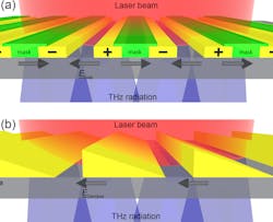
A specially designed photoconductive terahertz emitter overcomes these problems by using a metal-semiconductor-metal (MSM) interdigitated finger structure processed by optical or electron beam lithography. A simple array of interdigitated biased metallic stripes would lead to destructive interference of the generated radiation in the far field since the electric field changes sign in every gap between the fingers. Hence it is important to mask every other gap between two electrodes (see Fig. 1a). This results in a coherent superposition of the generated terahertz radiation in the far field due to unidirectional acceleration of the carriers over the entire illuminated active area.6 The size of the active area can be up to 10 × 10 mm2, and the electrode widths and spacings are chosen to be 5 µm. These small gaps ensure that an acceleration field on the order of several tens of kilovolts per centimeter is easily obtained with a simple power supply.
Photo-Dember effect
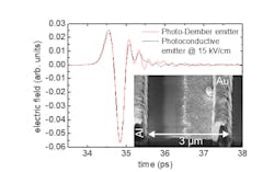
Recently, a new concept for terahertz emitters based on the lateral photo-Dember effect was realized.7 These emitters do not need an external bias. Instead, the driving force for the time-dependent polarization is a lateral gradient in the optically excited carrier density. Such a gradient results in ultrafast diffusion currents of electrons when exciting the edge of an opaque material covering a semiconductor. The faster diffusion of electrons into the non-excited area compared to the slower hole diffusion builds up a space-charge field (that is, the lateral photo-Dember field). Analogous to the interdigitated photoconductive emitters a simple array of metallic stripes would lead to destructive interference, because the two carrier gradients of every metal stripe point in opposite directions. By breaking the lateral symmetry of the opaque stripes through a thickness variation of the metal every other carrier gradient can be suppressed, resulting in a unidirectional carrier gradient over the entire active area (see Fig. 1b).The measured terahertz electric fields of a photo-Dember emitter and an interdigitated photoconductive emitter with an accelerating field of 15 kV/cm were compared using a rapid-scanning terahertz precision spectrometer (see Fig. 2). While the photoconductive emitter is made on semi-insulating GaAs, the photo-Dember emitter is prepared on an epitaxial layer of In0.53Ga0.47As grown on an indium phosphide (InP) substrate. Due to the smaller bandgap energy of InGaAs (0.74 eV) compared to GaAs (1.42 eV), the photo-Dember emitters can be also used in combination with a compact erbium-doped femtosecond fiber laser.8
Radio frequency bias
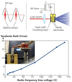
A different way to increase the size of the emitter uses a radio frequency (RF) bias.9 The trap-enhanced fields exist only when carriers are injected electrically, from the electrode into the semiconductor. It was found that by using an RF field with a frequency near the repetition rate of the laser to bias the emitter, a uniform bias field could be produced inside the semiconductor that was sufficient to generate terahertz radiation, even with an insulating layer between the metal electrodes and the semiconductor. The RF bias can be passively enhanced using a tank circuit, so that high-voltage electronics are not required (see Fig. 3). By synchronizing the RF bias to the repetition rate of the laser, an effectively constant (dc) field can be produced, or one can use a frequency slightly off the repetition rate, which allows lock-in detection at the difference frequency. Emitters using an RF bias and insulated electrodes were found to be extremely robust against damage by the intense laser field and large bias field, a common problem in photoconductive emitters. The terahertz emission showed no sign of saturation with increasing bias, suggesting room for improvement if the bias field can be enhanced further.In summary, recent advances show that a mature technology, the photoconductive ultrafast terahertz source, still has room for improvement and will continue to be an important method for generating terahertz radiation.
REFERENCES
1. D.M. Mittleman, ed., Sensing with Terahertz Radiation, Springer (2003).
2. C.A. Schmuttenmaer, Chem. Rev., 104, 1759 (2004).
3. A. Bartels et al., Rev. Sci. Instrum., 78, 035107 (2007).
4. P.R. Smith, D.H. Auston, and M.C. Nuss, IEEE J. Quantum Electron., 24, 255–260 (1988).
5. J.H. Kim, A. Polley, and S.E. Ralph, Opt. Lett., 30, 18–20 (2005).
6. A. Dreyhaupt et al., Appl. Phys. Lett., 86, 121114 (2005).
7. G. Klatt et al., Opt. Exp., 18, 4939 (2010).
8. G. Klatt et al., Appl. Phys. Lett., 98, 021114 (2011).
9. H. Zhang et al., Opt. Lett., 36, 223–225 (2011).
Jared Wahlstrand is senior research associate at the Department of Physics, University of Maryland (College Park); Thomas Dekorsy is professor at the Center for Applied Photonics, University of Konstanz (Konstanz, Germany); Gregor Klatt is a product development engineer at Gigaoptics GmbH (Konstanz, Germany); and Steven Cundiff is a Fellow at JILA, National Institute of Standards and Technology and University of Colorado (Boulder, CO); e-mail [email protected].


