HIGH-SPEED DETECTORS: Ultracompact 45 GHz Ge photodiode features ultralow energy consumption

To maintain the bandwidth demands for future communications networks, integrated-photonics architectures based on silicon photonics and other semiconductor platforms are being developed at numerous research institutions. A necessary component recently developed by researchers at Sandia National Laboratories (Albuquerque, NM), IQE Silicon Compounds (Cardiff, England), and the Massachusetts Institute of Technology (MIT; Cambridge, MA) for Sandia’s complementary metal-oxide semiconductor (CMOS)-compatible silicon-photonics process is an ultracompact, high-speed germanium (Ge) photodiode with a 1.2 fF ultralow intrinsic capacitance—so low that it could enable direct driving of a transistor gate, eliminating the need for a transimpedance amplifier (TIA), drastically reducing power consumption in next-generation communications links.1
Bottom-up approach
Unlike typical fabrication processes for Ge photodiodes on silicon in which blanket epitaxy is used to grow layers followed by lithography and etching steps to remove material, the researchers instead used a bottom-up approach in which Ge is grown selectively in oxide windows. The bottom-up approach reduces the density of dislocations in the detector structure, as the dislocations that do form can terminate at the window edge, leading to an overall reduction in dark current.
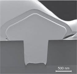
The photodiode fabrication steps include selective in situ growth of Ge doped with boron in an oxide trench on top of a silicon pedestal (see figure). The Ge is overgrown prior to chemical-mechanical polishing (CMP) to complete the waveguide planarization process for a final Ge thickness targeted at 0.6 μm. Phosphorus is implanted to form the n-type layer and top contact of the photodiode, followed by deposition of a capping oxide to complete the vertical n-i-p structure. After adding electrical contact features, a 2.5-μm-thick optical oxide cladding is added via plasma-enhanced chemical vapor deposition (PECVD).
Dark current, responsivity, 3 dB bandwidth, and noise-equivalent power (NEP) analysis on photodiodes fabricated with 1.3 to 5.3 μm waveguide widths and 4 to 64 μm lengths revealed that the lowest dark-current density of approximately 40 mA/cm2 at 1 V reverse bias increased linearly with waveguide width, but could be reduced to the order of 1 mA/cm2 if an additional anneal step were added to the fabrication process in order to further reduce dislocation defects. And although responsivity improved for larger waveguide widths and lengths, the increase in dark current increased shot noise more rapidly than the responsivity, creating less sensitive photodiodes with a higher NEP. Consequently, smaller photodiodes are more sensitive and have lower intrinsic capacitance.
'Ultra' performance
Unlike other demonstrations of Ge on silicon photodiodes in this class with dimensions on the order of 60 μm2, an ultracompact bottom-up fabricated Ge photodiode with dimensions of only 5.2 μm2 (1.3 × 4 μm) exhibited a 45 GHz bandwidth at 1 V reverse bias, 3 nA dark current, and 0.8 A/W responsivity. And with a 37 GHz bandwidth at 0 V reverse bias and 30 μA of photo-current, the devices are definitely amenable to high-speed operation at CMOS driving voltages.
"Sandia National Laboratory has established a long history of leadership in high-performance computing (HPC)," says Christopher T. DeRose, senior member of technical staff at Sandia National Laboratory. "A critical technology for future HPC systems is ultralow-power optical communication links connecting the CPUs of the machine. Extremely high bandwidth and low capacitance (femtofarad) germanium photodiodes will ultimately enable sub-100 fJ/bit optical communication to become a reality."
REFERENCE
1. C.T. DeRose et al., Opt. Exp., 19, 25, 24897–24904 (Dec. 5, 2011).

Gail Overton | Senior Editor (2004-2020)
Gail has more than 30 years of engineering, marketing, product management, and editorial experience in the photonics and optical communications industry. Before joining the staff at Laser Focus World in 2004, she held many product management and product marketing roles in the fiber-optics industry, most notably at Hughes (El Segundo, CA), GTE Labs (Waltham, MA), Corning (Corning, NY), Photon Kinetics (Beaverton, OR), and Newport Corporation (Irvine, CA). During her marketing career, Gail published articles in WDM Solutions and Sensors magazine and traveled internationally to conduct product and sales training. Gail received her BS degree in physics, with an emphasis in optics, from San Diego State University in San Diego, CA in May 1986.