CHARGE-COUPLED DEVICES: CCD imagers take new pixel approach for high-end applications
JAN BOSIERS, HOLGER STOLDT, PETER HARTOG, WILCO KLAASSENS, and NIXON O
While consumer requirements force manufactures of imagers based on charge-coupled devices (CCD) and complementary metal-oxide semiconductors (CMOS) to decrease the pixel sizes, the driving factor for professional applications is better image quality.
In mobile phones, CMOS imagers with pixel sizes as small as 1.45 × 1.45 µm are now entering the market. Because pixel size reduction allows higher sensor resolution without a significant increase in cost of the imaging module, the pixel race still dominates in this market. Typical chip sizes are smaller than 0.5 × 0.5 cm, with resolutions up to 5 megapixels.
At the opposite, high-end resolution, segment of the photography market, typical pixel sizes are about 7 × 7 µm with chip sizes as large as 36 × 48 cm, and resolutions up to 40 megapixels. Many of these professional applications use full-frame or frame-transfer CCD imagers. Technology developed for such high-end digital-still-camera applications is now being applied to improve CCD imagers for demanding medical and scientific applications.
High-end imaging requirements
Typically, high-end single-shot “static” applications in medical x-ray and scientific applications require large pixel sizes since they offer the required dynamic range of 12 bits or more. Large image formats, such as 24 × 36 mm or 36 × 48 mm, are often required to meet the optical system requirements. For continuous-video x-ray and scientific applications, speed (frames per second) and compatibility with existing lenses (a 1/2 in. format or 8 mm image diagonal) are key features.
In a conventional CCD imager, a three-phase full-frame CCD pixel comprises three layers of polysilicon (see Fig. 1). But by adopting a more simplified approach that was developed for professional digital still camera and high-definition television applications, a new pixel concept is available to improve imaging resolution and quality.
The challenge for the designer and technologist was to combine high quantum efficiency and large charge capacity with low dark current, good highlight-handling properties, and a high modulation transfer function (MTF). This was achieved by combining the “vertical overflow drain” pixel concept with a high fill factor and a high transmittance of the optical stack.
The VOD pixel concept
In the vertical overflow drain (VOD) concept, the CCD channel is formed as an n-channel implant on a p-well in an n-type substrate. This VOD technology (also called vertical antiblooming or VAB) is a preferred implementation for buried-channel CCD imagers with strict requirements on overexposure control and electronic shuttering.
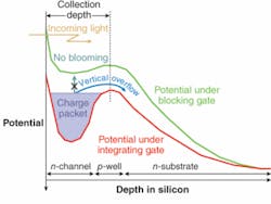
The VOD pixel structure can be conceptualized by the potential profile as a function of depth in the silicon, under an integrating and a blocking gate (see Fig. 2). The generated electrons are collected in the potential well. The vertical n-p-n structure limits the collection depth of electrons generated by incident photons to 2 to 3 µm deep inside the bulk silicon—that is, electrons migrate to the position of the local potential maximum (downward in the figure). This collection depth, in combination with the penetration depth of photons in silicon, results in a response curve as a function of wavelength similar to that of the human eye. When a highlight in the scene generates more electrons than can be stored in the pixel, the excess charge is drained to the substrate, and does not bloom into neighboring pixels because the potential barrier to the substrate is lower than the potential barrier to a neighboring pixel.This concept also makes electronic shuttering very easy to implement. To start the exposure, all gates are first set to “low” and a pulse is applied to the n-substrate for a short time. This removes the local potential maximum in the pixel, and all electrons are drained to the substrate. Then the charge collection can start. In imagers without VOD, the charge first has to be transported out of the imager, which takes time and requires additional power.
The four electrodes that define a pixel are made of two layers of adjacent (or nonoverlapping, as in conventional CCDs) very thin, transparent-membrane polysilicon layers. This ensures a very high transmission of light and a planar structure that is beneficial for good quantum efficiency. The electrodes are connected to narrow metal straps, running above the p+ channel stops, to ensure low RC time constants. Together with the small “overlap” capacitance between neighboring electrodes, this makes the technology ideally suited for high speeds. A four-phase pixel implementation was chosen because it offers the highest charge storage capacity per unit area, and because it allows bidirectional transport.
A major advantage of this simple yet powerful concept is the intrinsic high fill factor (without the use of on-chip microlenses, often undesirable in medical or scientific applications) of more than 90%. Combined with the transparent electrodes and vertical antiblooming, this concept results in a delicate balance of high quantum efficiency combined with a very wide, symmetrical angular response and a high MTF. The vertical antiblooming concept also results in a low dark current because any dark current generated in the bulk of the device (in the n-substrate below the potential minimum) is not collected in the pixel.
The combination of low capacitance and metal straps allows for very high transport speeds—frame shift (vertical) frequencies up to 10 MHz and readout (horizontal) frequencies up to 130 MHz have been demonstrated. Even an imager capable of capturing images at 1 million frames per second (fps) was realized using this technology.
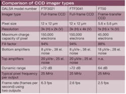
Finally, this technology also allows the design of low-noise, high-speed output amplifiers. A noise level as low as 10 electrons (after conventional correlated double sampling to remove the reset noise) is achieved on imagers for professional digital still camera applications with amplifiers operating at 25 MHz pixel frequencies and bandwidths up to 130 MHz, with a charge handling capacity in excess of 50000 electrons (see table).Applications
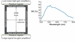
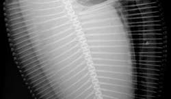
DALSA Professional Imaging has developed a 3k × 4k CCD imager with 12 × 12 µm pixels that uses all the features of this new technology (see Fig. 3). By using the bidirectional transport capabilities in both the image array and the readout register, this imager can be read either through one or two amplifiers of either the top or bottom readout register—user selectable by applying the appropriate clock pulses. The “top” amplifiers are optimized for low noise in applications that require the detection of small-to-medium charge packets (up to 80,000 electrons), by using a low charge-to-voltage capacitance at the detection node. The “bottom” amplifiers are optimized for applications where high charge capacity is more important. This option can be very interesting for medical or scientific applications that are x-ray photon shot-noise limited (see Fig. 4). To achieve the required matching between charge handling of the pixels and the chosen amplifiers, the charge capacity in the pixels can easily be tuned during integration by adjusting the image electrode voltages.Using this same technology, a 1/2 in. 1k × 1k frame-transfer CCD with 5.6 × 5.6 µm pixels and split readout through two outputs achieves a dynamic range of 64 dB at 30 fps. Operation at 100 fps is possible with a pixel frequency of 2 × 60 MHz.
For those medical and scientific applications that require extremely high quantum efficiencies and large imager sizes, a 2k × 2k CCD with 24 × 24 µm pixels was developed using the same technology, but using an n-channel buried CCD in a p-type substrate, instead of a three-layered n-p-n structure. The absence of a vertical overflow drain removes the overexposure control option, but significantly increases the collection depth, resulting in higher QE values for green and red light. A QE as high as 65% for green and 75% for red was achieved.
Jan Bosiers is R&D director, Holger Stoldt is program manager R&D, Peter Hartog is project leader, and Wilco Klaassens is technology scientist at DALSA Professional Imaging, High Tech Campus 27, M/S 14 (WL01), 5656 AE Eindhoven, The Netherlands; e-mail: [email protected]; www.dalsa.com/pi. Nixon O is technical director, DALSA Digital Imaging, 605 McMurray Rd., Waterloo, ONT, Canada.


