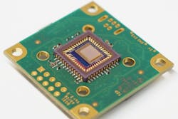
Spectrometers: Single-shot on-chip spectrometer is candidate for integration into smartphones
Engineers at the University of Wisconsin-Madison have developed a single-shot spectrometer that is so small and simple that it could integrate with the camera of a typical cell phone without sacrificing accuracy. The device contains photodetector arrays overlaid with photonic-crystal (PC) slabs placed on top of the detector pixels, with each PC slab having a different spectral response (see figure).1 The individual spectral responses are complicated and finely patterned (“random” spectral filters) and an algorithm is used to extract the spectral profile of the incoming light. Other potential uses include health-care devices, and compact manufacturing monitors.
The spectrometer is based on a type of spectral response that is different from most spectrometers. Typical spectrometers rely on one of two spectral-response approaches: monochromator and Fourier-transform. A grating, microcavity, or prism spectrometer uses its spectral dispersion as a monochromator, enabling it to sample the spectrum point-by-point. A Fourier-transform spectrometer has a sinusoidal spectral response that is varied to produce the data, which is then processed via a Fourier analysis. The new spectrometer uses neither of these approaches—instead, the PC slabs have complex spectral responses that are a result of the particular PC structures themselves. The test spectrum is recovered using either a least-square or compressive-sensing method.
The PC slab overlaying the image sensor has 36 different square PC structures, each 32 × 32 µm on a side; the total size of the spectrometer is 216 × 216 µm. The researchers designed the different PC structures so that the correlation between the different spectral responses was at a minimum. Electron-beam lithography was used to create the differing PC nanopatterns. In general, using this technique, the more individual PC slabs are used, the higher the resolution, but the larger the size of the sensor.
To have both high spectral sensitivity and large bandwidth, conventional spectrometers usually must be relatively large with a long optical path length. The new spectrometer is small and thin enough to lie directly on a sensor from a typical digital camera. “This is a compact, single-shot spectrometer that offers high resolution with low fabrication costs,” says Zhu Wang, one of the researchers.
The researchers say that the PC slabs force incoming light to bounce back and forth several times before reaching the sensor, elongating the path length without adding bulk, boosting the devices’ resolution. The instrument has a spectral range of 550 to 750 nm and a resolution of 1 nm.
Hyperspectral version
The researchers also created a configuration suitable for hyperspectral imaging by fabricating a 10 × 10 array of spectrometers on a silicon-on-sapphire substrate. Overlaid on a CMOS sensor, it formed a 100-pixel hyperspectral imager. Even with the limited resolution, it easily distinguished and spectrally characterized numerals illuminated at different wavelengths to a 1 nm spectral resolution.
It should be noted that the spectrometer, and indeed the device’s hyperspectral configuration, are fabricated using standard CMOS fabrication techniques. The researchers say that the number of pixels in their prototype hyperspectral imager was limited by the lithography technique they were using, and that using high-throughput photolithography would allow them to extend the resolution of their present design to hundreds of pixels in each dimension, or 10,000 pixels or more in total.
Next, the team hopes to boost the device’s spectral resolution as well as the resolution of the images it captures. Ways to do this include using silicon nitride or silicon carbide instead of silicon, which the researchers say would create more diverse spectral features due to the lack of light absorption.
REFERENCE
1. Z. Wang et al., Nat. Commun. (2019); https://www.nature.com/articles/s41467-019-08994-5.

John Wallace | Senior Technical Editor (1998-2022)
John Wallace was with Laser Focus World for nearly 25 years, retiring in late June 2022. He obtained a bachelor's degree in mechanical engineering and physics at Rutgers University and a master's in optical engineering at the University of Rochester. Before becoming an editor, John worked as an engineer at RCA, Exxon, Eastman Kodak, and GCA Corporation.
