Innovation should play a meaningful role for any industry—but there is something special about each innovation within the photonics and optics realm. After all, each innovation within this space enables other industries to take the next step.
This year’s submissions are no exception. There are some truly groundbreaking innovations that will ultimately change the many products impacting our daily lives for years to come. Everyone on this list deserves recognition.
Each submission goes through the same process, judged by an impartial panel focused on the level of innovation and its perceived benefit to the further evolution of the industry.
And now, on to the honorees...
PLATINUM-LEVEL HONOREES
ams OSRAM and Jabil
1130 nm VCSEL for SWIR 3D Camera
ams OSRAM has developed laser sources that are suitable for both indoor and outdoor 3D sensing applications. Designed at the specific emission wavelength of 1130 nm in the form of a vertical-cavity surface-emitting laser (VCSEL), it is able to detect and image objects up to 20 m in distance with Z-accuracy of less than 1%. This technological advancement is beneficial for imaging in environmental conditions with high levels of ambient light, where the interference by the solar irradiance typically causes high temporal noise levels on the captured image.
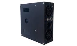
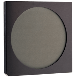
ams OSRAM, Jabil, and Artilux combined their proprietary technologies in semiconductor lasers, 3D sensing architecture design, and germanium-silicon (GeSi) sensor arrays based on a scalable complementary metal-oxide-semiconductor (CMOS) technology platform, respectively, to demonstrate a 3D camera that operates in the short-wavelength infrared (SWIR), at 1130 nm. The 3D camera is based on the indirect time-of-flight method with modulated light emitting at 1130 nm to calculate the distance to an object (see Fig. 1).
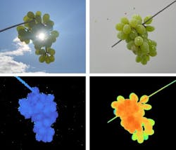
The performance of the camera in detecting objects in three conditions - indoors, outdoors with sun facing the target, and outdoors with sun facing the camera - demonstrates that, with an 80% reflectivity target located at the distance of 20 m, the detection accuracy was less than 1%. Figures 2 and 3 show the application of the 3D camera using the 1130 nm laser light source in capturing images under all three environmental conditions, demonstrating the ability of the proposed technology to provide robust 3D depth profile images of target objects.
These 1130 nm laser devices are grown on low-cost gallium arsenide (GaAs) substrates using the conventional metal-organic chemical vapor deposition (MOCVD) technique and are based on a lattice-matched indium gallium arsenide (InGaAs)-based active light-emitting material system. Therefore, the total cost of producing such laser devices is significantly lower compared to other SWIR laser sources with similar performance characteristics but emitting at different wavelengths, such as 1380 nm. These sources are typically based on indium phosphide (InP) substrates and dilute-nitride active light emitting material system. Additionally, in contrast to the 1380 nm laser source, which is absorbed by human skin and could lead to unusable data for depth sensing, the 1130 nm laser source mostly reflects light from the skin, resulting in a clear 3D image. Moreover, 1130 nm laser devices are more eye-safe, with approximately twice the safety margin of 940 nm laser sources. The 1130 nm laser technology developed by ams OSRAM and utilized by Jabil demonstrates the ability of 3D imaging in both indoor and outdoor environments with high image detection accuracy.
Edmund Optics
PeakPower High LDT Low GDD Ultrafast Mirrors
The PeakPower High LDT Low GDD Ultrafast Mirrors from Edmund Optics use an innovative design approach to maximize laser damage threshold (LDT) for ultrafast pulses. They have the highest available laser damage threshold for thin film coatings designed for 920 nm ultrafast lasers, with LDT values exceeding 0.75 J/cm2 for 25 fs pulse durations at 920 nm. The PeakPower Mirrors boast a group delay dispersion (GDD) of 0 ±50 fs2 @ 45° angle of incidence (AOI) over a broad spectral bandwidth of 830–1010 nm, letting them prevent chromatic dispersion and pulse spreading in the most demanding ultrafast applications. A 45° AOI makes them perfectly suitable as turn mirrors in advanced ultrafast laser systems. These mirrors' high reflectivity of Rs > 99.50% @ 830–1010 nm @ 45° AOI ensures minimal loss while maintaining ultrashort pulse durations. The outstanding LDT values ensure they will perform even under exceptionally high ultrafast pulse energies.
More applications are moving to the short pulse durations of ultrafast lasers for their higher peak powers and minimized damage to surrounding areas in applications like materials processing and medical surgery. The PeakPower Mirrors enable these ultrafast systems to drive towards even higher powers and push the ultrafast market to new territories.
Gentec Electro-Optics
QE195LP-S-MB-QED-D0 energy meter for large beams up to 700 J
Research with high-energy lasers is crucial for challenges such as green nuclear power production and a better understanding of fundamental light-matter interactions, propelling a host of discoveries in nuclear physics, medicine, and environmental sciences. Major facilities like the Extreme Light Infrastructure (ELI), the National Ignition Facility (NIF), the Center for Relativistic Laser Science (CoReLS), the Zettawatt Equivalent Ultrashort pulse laser System (ZEUS), and the Apollon laser facility, to name a few, are pushing the boundaries of the world’s most intense lasers.
Historically, record-breaking laser intensities have primarily been achieved with shorter, but infrequent pulses. In the past decade, scientists have managed to increase the repetition rate of shots in these large laser chains. Where a few years ago the high-energy systems could only fire a pulse every few minutes, we now have petawatt-level facilities that operate at tens of pulses per second, and projects are in the works for systems that will run at hundreds of pulses per second.
These high-intensity, high-repetition-rate laser systems come with multiple challenges for the scientists who design and operate them. The laser pulses must be thoroughly characterized, for three important reasons: 1) to demonstrate the ground-breaking records, 2) to improve the laser systems’ stability and repeatability, and 3) to support the research experiments that are done with these lasers. But how can these pulses be measured? There is a rising need for measurement instruments to characterize these high-energy laser pulses with repetition rate. Before launching this new product, calorimeters could be used, but since they were limited to a single shot at a time, users had to wait several minutes for the detector to stabilize before the next measurement. Since researchers are at the limit of current technologies, these systems have stability challenges, and therefore they need to test and characterize the systems accurately. Therefore, there is a need to measure all pulses with precision and traceability.
Also, given that these users work with very high energies and very powerful amplification, their systems are designed with large beams, and the detector surface dimension quickly becomes a limitation. They need detectors with very large apertures to accommodate their extra-large beams. Gentec’s new large-aperture joulemeter measurement instrument meets all these needs, so it can help researchers continue to push the boundaries of high-energy laser science and help them continue their very important research in the study of light-matter interactions and nuclear fusion. This innovation therefore increases productivity for materials processing and energy production by eliminating the long wait time between each measurement. It also decreases the research time in all industries using extra-large beams. Simply put, measuring extra-large beams has become more convenient for everyone.
LEADOPTIK
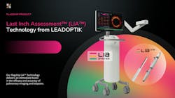
LIA: Last Inch Assessment
According to the American Cancer Society, the mortality rate for lung cancer in the U.S. exceeds that of the next three cancers combined. Diagnosing peripheral pulmonary lesions is particularly challenging due to their size and location, often resulting in inconclusive biopsy results. This necessitates repeated biopsies in 60% of cases and leads to delayed treatment. Current biopsy procedures suffer from a lack of real-time visualization capabilities, resulting in suboptimal targeting and sampling errors. The LIA (Last Inch Assessment) system offers a breakthrough solution by integrating depth imaging technology directly into biopsy needles. This enables real-time, high-resolution imaging of lung tissue during the biopsy procedure. By empowering clinicians to precisely target and sample suspicious lesions, the LIA system improves diagnostic accuracy and reduces the necessity for repeat procedures.
GOLD-LEVEL HONOREES
ams OSRAM
8-Channel 915 nm SMT Pulsed Laser in QFN package
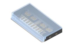
ams OSRAM’s new SPL S8L91A_3 A01 is an infrared high-power SMT laser designed for light detection and ranging (LiDAR) applications, featuring a single monolithic die with 8 channels of 915 nm pulsed laser in a QFN package. Capable of delivering 1000 W peak optical power from a single package, this impressive output power meets the requirement of long-range, high-resolution LiDAR sensors for autonomous highway driving using a single laser package. By using a single packaged laser, customers can develop more streamlined and compact LiDAR sensors, while also eliminating the concerns of alignment and tolerances and the need to perform their own die and wire bonding, thereby simplifying manufacturing processes and reducing time to market. Additionally, the laser incorporates ams OSRAM’s proprietary wavelength stabilization technology, which significantly reduces wavelength shift over temperature. As a result, this enhances the LiDAR sensors’ signal-to-noise ratio by reducing the filter width at the detector, further extending the detection range. Furthermore, this product is backed by rigorous testing surpassing AEC-Q requirements, ensuring reliability to meet stringent demands of automotive OEMs. This new product joins ams OSRAM’s existing single and 4-channel SMT laser family, with a proven track record on the street. ams OSRAM has been a market leader in the development and production of pulsed infrared lasers for automotive LiDAR for over 20 years. There are now more than ten million units in the field—without a single chip defect. SPL S8L91A_3 A01 is the newest addition to the product lineup and is built on that extensive experience in automotive LiDAR technology.
EssentOptics Europe UAB
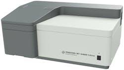
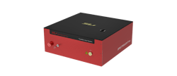
PHOTON RT 0420 Ultra Spectrophotometer
Exceptional optical coatings demand exceptional metrology. The newest PHOTON RT 0420 Ultra spectrophotometer addresses the longstanding challenge of characterizing cutting-edge multilayer optical coatings, including ultra-narrow bandpass filters, cut-off filters with steep slopes, notch filters, and coatings with high optical density. Until now, vacuum deposition technologies have outpaced available metrology solutions. Optical coaters have gained access to the latest generation of highly advanced sputtering technologies, such as ion-beam sputtering and magnetron sputtering, potentially enabling them to design and produce exceptional optical coatings. However, the lack of specialized high-performance spectrophotometers prevents them from making a full-fledged qualitative leap in bringing such coatings to market. This, in turn, leads to slower advances in critical market segments such as LIDAR, fluorescence microscopy, laser safety, optical data transmission, space exploration, Earth observation, and next-level defense and security applications. The proven quality of optical coatings is directly correlated with the measurement accuracy of the spectrophotometer.
With the PHOTON RT 0420 Ultra spectrophotometer, EssentOptics offers a high-accuracy and application-focused metrology solution directly to coating professionals. Its knowledge-intensive spectrophotometer will facilitate both research and production of new coating designs, significantly reducing the time-to-market for photonics instruments with advanced coatings. The PHOTON RT 0420 Ultra spectrophotometer not only successfully meets current metrology challenges, but also inspires coating experts to design and produce sophisticated thin-film stacks. With its powerful and user-friendly features, achieving success is no longer just a dream.
Laservision
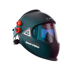
Panoramaxx Laser Welding Helmets
Laser welding is an important technology with great potential and an indispensable tool for high-quality and cost-effective production. This is particularly important in applications where tight tolerances and minimal distortion are required, such as in aerospace or medical technology. The market for hand-held welding laser systems, which is developing explosively due to the technological progress of laser technology, especially fiber lasers, is making a decisive contribution to the further spread of laser technology in ever new areas. Therefore, end users are the greatest benefactors of the Panoramaxx laser welding helmets. The versatility presented by this hybrid solution offers welders a streamlined option while maintaining the highest level of protection. In addition, the comfort level provided exceeds other user experiences due to the innovative Iso-fit system. Furthermore, the helmet design offers the user a greatly improved field of vision making the product not only the most comfortable, but best for precise and error-free work.
LightPath Technologies
BDNL Black Diamond Chalcogenide Glasses
Infrared optical systems are becoming increasingly relevant in today’s military environment. The advancements in processing power, machine learning, and semiconductors has had a side effect, allowing any nation state with access to graduate-level university talent and commercially available hardware to develop very sophisticated active and passive RF capabilities. This escalating worldwide “ECC….CM” environment has increased the utility and importance of infrared (IR) solutions used in the detection and tracking of threats and targets.
Germanium (Ge), a natural ore, is a critical material used in refractive optical applications in midwave (MW) and longwave (LW) IR systems. Germanium's high demand is because it is one of a handful of optical materials that pass both MW and LW and can withstand tactical military environments. Unfortunately, the source of the Ge ore and pre-processed Ge used in the vast majority of Ge blanks sourced from companies in the U.S. and stable European partners comes from Russian and Chinese mines. Exciting developments in chalcogenide glasses produced by LightPath, leveraging the initial developments made by Naval Research Labs (NRL), have the potential to replace Ge in many DoD applications. This family of chalcogenide glasses contain small amounts of Ge or no Ge, and therefore its constituents do not depend on potentially unstable sources. As a side benefit chalcogenide glasses, as they are mixtures, can be tuned for passband, refractive index, and dn/dt. Additionally, chalcogenide glasses can be net shape molded into lenses, including asymmetric aspheres to greatly reduce the cost of optical elements.
LightPath, a Florida-based small business, is supported by the Defense Logistics Agency and NRL to produce and also qualify these chalcogenide glasses as alternative materials to germanium. Until now, lenses have not been able to transmit IR lighting without the use of crystal glass, which represents significant supply chain issues and complexities in manufacturing. LightPath’s BDNL Black Diamond glass allows designers to utilize a variety of optical applications while minimizing the use of crystal glass, and allows for the design of much more compact and complex systems. These materials are bringing a new level of innovation to IR imaging that until now did not exist.
Lumotive
LM10
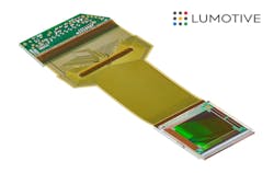
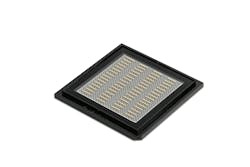
LM10 is Lumotive’s first production offering of their groundbreaking Light Control Metasurface (LCM) technology, which provides truly solid-state digital beam steering for superior optical 3D sensing performance. As an optical semiconductor made using widely-adopted silicon manufacturing processes, LM10 overcomes all the cost, size, and reliability limitations of traditional mechanical LiDAR.
Lumotive's LCM technology is revolutionizing LiDAR with the introduction of the world's first mass-producible, commercially available solid-state beam steering solution. Unlike traditional beam steering based on some form of moving polygons or mirrors, Lumotive’s dynamic optical metasurfaces offer far superior control over light manipulation. LCMs are compact, lightweight, and remove the need for mechanical parts, paving the way for greatly improved performance and reliability over existing 3D sensing techniques.
The LM10 chip marks a significant departure from conventional 3D sensing and LiDAR technology. Unlike traditional mechanical beam steering, which is prone to inaccuracies over time and use due to the presence of moving parts, the LM10 chip is purely solid-state, ensuring higher precision and greater reliability. Its modularity also makes it highly adaptable, allowing for easy integration with a range of LiDAR use cases. LM10’s production employs standard silicon CMOS manufacturing techniques, tapping into the existing economies of scale within the semiconductor industry. This strategy not only guarantees a cost-effective product, but also facilitates straightforward scalability for mass production. Lumotive achieved this innovation without the need for exotic or prohibitively expensive materials, meaning the technology can be globally adopted and deployed. As the first company to commercialize dynamic optical metasurfaces in 3D sensing, Lumotive is setting new industry benchmarks for performance, reliability, and versatility.
The LM10 chip’s innovative design delivers superior precision and durability compared to existing LiDAR systems. Whereas mechanical beam steering suffers from unreliability due to the inherent limitations of moving parts, semiconductor-based LCM technology steers laser light photonically to precise, repeatable, digitally controlled steering angles. This solid-state approach enables compact, reliable solutions with enhanced accuracy and dramatically reduced maintenance needs—ideal traits for autonomous vehicles, smart infrastructure, next-generation cinematographic equipment, and other cutting-edge applications where 3D sensing interacts with the physical world. LM10's software-defined beam steering also allows customizable scan patterns optimized for specific use cases. This enables a sensor to reallocate the time spent at each steering angle to create an arbitrary number of regions of interest in any size and configuration. For example, an AMR can switch between long- and short-range scanning based on its need to navigate or scan cargo, or an autonomous vehicle can change from a long and narrow field of view to a short and wide one when it slows at an intersection.
Lumotive provides LM10 partners with a complete reference design, including algorithms and manufacturing processes, empowering rapid commercialization of LCM-based 3D sensors tailored to any application. By replacing outdated mechanical lidar with field-proven programmable photonics, sensor makers can bring high-performance 3D sensing solutions to a wider range of markets and market segments, and still do so quickly and efficiently. With its combination of precision, resilience, and adaptability, LM10 is ushering in a new era of LiDAR, which is ready to take over the 3D sensing market.
OZ Optics Ltd.
Two-Qubit Polarization Entanglement Analyzer
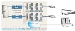
OZ Optics is excited to offer a two-qubit polarization entanglement system. It represents a cost-effective analyzer that reduces the complexity level, effort, and cost to perform one of the most precise polarization entanglement analyses using two detectors. This analyzer, along with a control system, features plug-and-play operation. Moreover, it is supplied with optional software to perform a set of 36 measurements in the canonical basis {H, V, D, A, R, L} ⊗ {H, V, D, A, R, L} for generating precise tomography using two single-photon detectors in the course of a quick experiment.
OZ Optics exclusively offers such plug-and-play analyzers. Photon pairs of a given polarization-entangled photon source can be precisely analyzed with a negligible insertion loss. This system allows for quick quantum analysis while controlling the polarization states of the photon pairs with high precision. This is achievable through built-in encoders enabling closed-loop operation. The coincidences rate distribution, which is the core of reconstructing a photon pair polarization state, can be measured at high precision and excellent repeatability over the course of a quick experiment.
SemiNex Corporation
High Power Gain Chip Array for AI Computing and Data Center
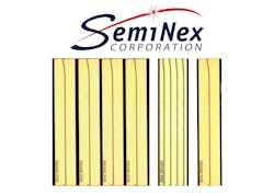
SemiNex Corporation proudly presents the industry-leading Gain Chip/Reflective Semiconductor Optical Amplifier (RSOA) platform that exhibits the best performance at both 1310 nm and 1550 nm wavelengths operated in the wide temperature range. The Gain Chip/RSOA structure is based on a proprietary AlInGaAs material system and advanced curved waveguide design with multiple quantum wells on InP substrate with excellent optical and thermal performances. With the high-performance Gain Chip/RSOA and advanced Array, external cavity lasers (for both fixed wavelength and tunable) and comb frequency lasers with high power and narrow linewidth can be achieved. The Gain Chip/RSOA platform can provide a single channel or an array beyond 20 channels. Such high channel count and customizable channel pitch, 127 µm for example, allow the system designers the freedom to integrate the Gain Chip array with a silicon photonic integrated circuit (PIC) to minimize the total footprint of the final system and to reduce the overall cost. As applications for high-power computing in AI and I/O interfaces in data centers demand ever-increasing optical power, the SemiNex Gain Chip/RSOA Array platform can help system designers to reach their desired targeted specifications and spearhead the next generation of photonics systems.
Spectrolight, Inc.
Tunable Laser System
Spectrolight’s tunable laser system (TLS) is an innovative, continuously tunable one-box laser system that combines a supercontinuum laser and Flexible Wavelength Selector (FWS: tunable bandpass filter) based on TwinFilmTM technology. TLS is the world's first picosecond tunable laser system covering the visible to SWIR range.
The main advantages of TLS are broadband continuous center wavelength and bandwidth (FWHM) tuning, high average power, easy control, low maintenance, and price. TLS has ultra-broadband wavelength tuning capability up to SWIR (410–1700 nm) with a precision of 1 nm and can control the FWHM 2 to 15 nm (nominal). High output power (>5 mW/nm [average]) can be produced with very high throughput compared to methods using nonlinear optics such as OPA. TLS does not require difficult alignments or adjustments, and the center wavelength and bandwidth can be controlled in real time using dedicated software. It can be applied to a variety of purposes at a relatively low price, and various models are available depending on the output power.
TLS has TLS-Red and TLS-Blue models, depending on the difference in bandwidth control function. TLS-RED can produce wide wavelength ranges of approximately 400 to 1700 nm and has a controllable FWHM of 2 to 15 nm (nominal), and TLS-BLUE has the same wide wavelength ranges with fixed FWHM at 10 or 20 nm. TLS-RED is suitable for fields that require precise scanning, and TLS-BLUE is ideal for fields that require high output power.
Spectrolight's TLS allows users to freely select the output power and wavelength ranges according to their needs. TLS has customized models, and depending on the application, users can choose from supercontinuum laser models and the variable wavelength range of FWS. TLS can be applied to various applications due to its broadband wavelength tunability. For example, TLS can be applied as an excitation light source in fluorescence microscopy. There are more than tens of thousands of types of dyes used in fluorescence microscopy, but optical excitation filters suitable for each dye are limited. TLS enables the best fluorescence imaging by using the optimal wavelength of the fluorophore. And because TLS is a picosecond pulsed laser, it can be applied to time-resolved spectroscopy and microscopy, such as TCSPC and FLIM. TLS can be applied for inspection in various applications, including semiconductors, machine vision, pharmaceuticals, environmental monitoring, food and agriculture, forensics, art and artifact analysis, and material science. Spectroscopy and microscopy are powerful techniques for identifying and analyzing substances based on their interaction with light. TLS can be used as an important source of these technologies.
SILVER-LEVEL HONOREES
DRS Daylight Solutions
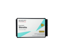
Stretto
DRS Daylight Solutions has launched Stretto, a family of high-precision lasers from UV to IR. Stretto, drawing its name from the musical concept of intricate overlapping, embodies precision and sophistication in laser technology. This advanced laser system offers unparalleled performance in UV, visible, and near-infrared spectrums. Stretto has been meticulously engineered as a versatile product platform, enabling expansion across a broad wavelength range while maintaining a uniform footprint and interface. This design philosophy not only facilitates scalability in various applications, but also ensures easy OEM integration without the need for extensive redesigns.
Stretto is ideal for industries that demand high precision and reliability, thanks to its efficient semiautomated manufacturing process. Setting new benchmarks in rugged laser technology, Stretto transcends the capabilities of standard external cavity diode lasers (ECDLs). It is a robust, compact, and lightweight solution, crafted to endure harsh environmental conditions, including humidity, dust, and extreme vibrations. This resilience makes Stretto uniquely suitable for challenging applications. In the rapidly evolving field of quantum technology, Stretto stands out with its resistance to temperature and pressure fluctuations, stability under extreme conditions, and an extensive mode-hop-free tuning range. It epitomizes the fusion of advanced engineering and adaptability, making it an indispensable tool for quantum sensors, clocks, and computing systems.
Lasers are the backbone of quantum information technology, and Stretto is at the forefront. It offers unmatched precision and control, essential for quantum computing, communication, and metrology. From laser cooling and trapping to scalability in quantum networks, Stretto provides the reliability and adaptability required for cutting-edge quantum applications. DRS Daylight Solutions is excited to offer Stretto to those pioneering in quantum research and applications, promising an unmatched combination of precision, flexibility, and resilience. Stretto is more than just a high-precision laser; it's a symbol of innovation in the realm of tunable lasers.
Duma Optronics
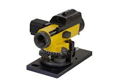
Total Station Autocollimator
Upgrades to these sensitive measuring devices expand their usability in photonics applications. Innovative enhancements of digital autocollimators enable a wide range of measurements for angular alignment, optical metrology, laser beam profilers, micro-alignment, augmented targets projection, multiwavelength, boresighting, and many more. Originally designed to measure angles, optical alignment, straightness, flatness, and parallelism, using a technique utilized in optical metrology for over a century, a digital autocollimator projects a collimated beam through an objective lens and captures the back-reflection from a mirror using the same objective lens, from which the term “autocollimation” is derived. The reflected image is then focused onto a charge-coupled device (CCD) detector. Through image processing and algorithms, this detector calculates the deviation between the initially projected beam and the incoming angular deviation of the reflected beam.
Modern high-tech industry presents unique challenges due to its intricate nature, integrating various technologies such as lasers, vision systems, computers, electronics, augmented and virtual reality (AR/VR) software, LiDAR, and more. New high-tech autocollimators aim to address the additional complexity by providing a comprehensive solution with multiple measurement capabilities integrated into a user-friendly electronic instrument. With this ‘Swiss army-knife’ inspired approach, the autocollimator has re-emerged as a leader in performance characterization for many photonics-related instruments. These applications span from AR/VR goggles and 3D LiDARs to satellite alignment and the inter-alignment of multiple optical elements combined with electronic sensors and lasers. The capabilities of this new instrument are extensive, encompassing optical and laser alignment, illuminated target projection, non-contact mechanical measurements in a plane perpendicular to its line of sight, laser characterization, laser and LiDAR characterization, power measurement, and distribution, among many others.
Due to high-level software package capabilities and its focus motorization feature, the system is applicable to all factory levels starting from scientific measurements, followed by characterization on development, enabling quality assurance measurement and alignment at the production level. Multifunctional autocollimators serve a wide range of applications in optical alignment, laser beam analysis, inter-alignment between optical elements, lasers, and mechanical components, as well as the analysis of complex photonic assemblies.
Omega Optical
DeepUV Transmission Grating
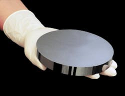
DeepUV Transmission TX Gratings from Omega Optical extend into the deep ultraviolet (DUV) at a reasonable cost. DeepUV transmission gratings were developed to provide fresh options in miniature, field-use spectroscopy, or medical applications, such as capillary analysis and HPLC. R&D engineers now have a manufacturable option at hand other than the historically available etched fused silica grating. This advancement in grating technology makes development and device production more affordable without compromising performance and field durability. Once a product design has been approved, DeepUV gratings are available in larger volumes greater than 1,000 per day, as this design is highly manufacturable and repeatable, and parts are delivered rapidly. How did Omega create such affordable yet high-performing gratings? By utilizing its foundational technology and deep understanding of material science to manufacture replicated gratings that offer affordable performance in the required spectrum, Omega Optical has a vast library of master gratings developed over the years, which allow the acceleration of product design when it is required.
Photonics Industries International, Inc.
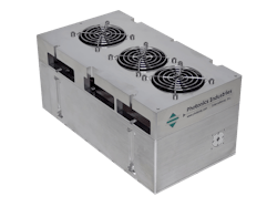
DP1k Series High Pulse Energy DPSS Nanosecond Lasers
The DP1k offers high pulse energy, TEM00 beam output, up to >15 mJ single pulse energy at 1 kHz pulse repetition rate in the infrared (IR) wavelength range, and high single pulse energy in the harmonic wavelength models as well, up to >12 mJ in the green, and up to >6 mJ in the UV. It offers exceptionally short pulse widths (~6–8 ns). The DP1k is exceptionally power-efficient, leveraging a novel diode-pumped configuration to ensure optimal energy use, Photonics Industries’ pioneering technology in intracavity harmonics for uncomplicated, true TEM00 output, and market-leading thermal management with air-cooling fans or radiative cooling techniques to adeptly manage the heat dissipation away from the laser head for stable operation. The DP1k is an all-in-one (AIO), compact package, with no separate chassis for a large power supply unit (PSU) or control utility module. Multiwavelength output options are available in the same-sized package, depending on the wavelength output requirement. The DP1k original and innovative design has allowed Photonics Industries to fulfill criteria in applications demanding low SWaP (size, weight, power consumption) while also needing high output pulse energy, TEM00 beam mode, and short nanosecond pulse widths. For example, the DP1k has fulfilled such needs/requirements in spectroscopy instrumentation and flat-panel display (FPD) microprocessing applications.
Suzhou Everbright Photonics Co., Ltd
50 W high-power semiconductor laser chips
Everbright is mainly engaged in R&D and production of high-power, high-brightness and high-efficiency semiconductor laser chips. A number of key breakthroughs have been made in core technologies such as chip design, MOCVD, lithography, cleavage/coating, package testing, fiber coupling, and so on; therefore, the power, brightness, efficiency, and reliability of the laser chip have been greatly improved. High-power, high-brightness, and high-efficiency semiconductor laser chips can be mass-produced.
Everbright launched a 9XXnm 50W semiconductor laser chip; the optical power increased 43% from 35 W to 50 W and the emitter width is 330 μm. The lateral structure is optimized and divergence angle is reduced. The brightness of the laser diode is increased significantly. As the laser chip's optical power increased, the pumping module power will increase proportionally. This will lead to higher optical power of the laser system such as the solid-state laser or fiber laser, and also reduce the price power ratio. The high-brightness feature of the laser chips enables the pumping module to have lower NA, and more optical modules can be coupled into the laser system, which also increases the power of the laser system. The feature will enable new applications, especially for those that need high brightness, such as thick plate cutting.
The high efficiency of the laser chips will reduce the waste heat, which will reduce the thermal load of the chiller in laser system. The wall plug efficiency of the custom laser system will increase and the total operating costs will be reduced. These means economic efficiency for the users. The high reliability of the laser chips will improve the lifetime of the laser system, and lower input in maintenance services after delivery. The high power, high brightness, high efficiency, and high reliability of the laser chips will enable laser systems with high power, high efficiency, high reliability, a lower price, and new applications.
TeraXion
LXM Narrow Linewidth DFB Laser Module
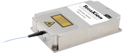
TeraXion leverages the key technological differentiators of a proprietary DFB laser diode with its new LXM narrow-linewidth laser module offering. Combining an intrinsically narrow laser chip with low-noise drive electronics and robust packaging, the LXM is a reliable and stable laser that provides low noise optical performances and unique frequency modulation properties. The module is operational from -20° up to 65°C.
The LXM module has been designed to fulfill the requirements of frequency noise sensitive optical systems that are usually deployed in industrial and/or critical monitoring context. In terms of performance, the LXM-U ultra-narrow model features a low frequency noise floor that sets new records in the category of single frequency lasers deployed in commercial systems. The unit emits light out of a monolithic semiconductor DFB laser that is slaved on a frequency discriminator. This approach ensures preserving the proven reliability and stability qualities of DFB laser diodes while boosting the end user’s system range and sensitivity. A model without frequency locking is also offered.
TeraXion’s DFB laser diode is intrinsically narrow (<25 kHz linewidth), and the native low level of frequency noise fulfills the requirements of many applications such as FMCW LiDAR, Doppler LiDAR, or few-kilometers-range fiber distributed sensing. The LXM-S standard module leverages this property under a direct-drive configuration to offer additional flexibility at a reduced cost. This model can be frequency modulated (FM) with high amplitude at a fast repetition rate while preserving its low phase noise performances. This translates into high spatial resolution and high data throughput for the end users. For system developers targeting mass markets, the LXM-S can be useful as a technology adoption vehicle. TeraXion’s DFB laser diode represents a small size narrow linewidth laser that can be scaled in volume at a low cost. The LXM-S reveals the potential of this technology when operated with reliable and stable through simple drive and modulation electronics. The 14 pins butterfly package integrated in the LXM-S will also be offered as a standalone product in the near future.
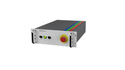
Finally, the LXM offering is a turnkey laser solution designed for flawless system integration. The laser is offered with an optional interface board for plug-and-play USB-C power and communication connectivity. A USB-C PD3.0 power block is also supplied, and each unit is factory-tested with its own power block. At any time, the interface board can be removed to allow the integrator developing its own control interface. In production phase, system integrators may prefer to purchase the laser alone to reduce size and cost. Different critical components are required to build a highly stable and reliable narrow linewidth laser that includes basic control functions: a single-frequency lasing medium and low-noise electronics such as a current source, a laser temperature controller, power management and communication electronics, locking electronics, and so on. The LXM main value proposition is to integrate everything in a small and rugged module such that a system integrator can rely on a highly performant light source and focus on what they do best: develop solutions that answer needs at the application level. Taking all the component considerations together, the LXM has been designed, benchmarked, and optimized as a whole to provide superior optical performance, reliability, and stability.
BRONZE-LEVEL HONOREES
3D-Micromac AG
microPREP PRO FEMTO
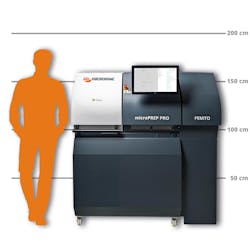
The microPREP PRO FEMTO laser micromachining system, developed by 3D-Micromac AG, is a groundbreaking innovation in high-speed Atom Probe Tomography (APT) and cross-section sample preparation. Traditionally, APT sample preparation processes have been based on electrolytic or ion-based thinning workflows. Both workflows require mechanical preparation steps that introduce mechanical stress to the specimen, which can affect the overall quality and yield. Using FIB milling for the preparation process to avoid mechanical stress can take many hours to complete and requires specialized lift-out of the specimen, which introduces the risk of damaging the specimen. Since FIB systems are costly, this approach also ties up FIB resources and results in very high operational costs for the user. Some systems combine a laser for high-speed ablation and an FIB for final polishing in a single platform. This approach creates capacity bottlenecks since only one process can be used at a time. In addition, since laser preparation ablates high volumes of material, particle contamination inside the analytic area of combination laser/FIB tools becomes a much bigger issue, and its removal is difficult due to the vacuum conditions inside the isolated laser or process chamber. Short pulse lasers can also cause large heat-affected zones (HAZs), which can not only damage the sample but also modify the structure of the probe tips, leading to inaccurate measurement results.
The microPREP PRO FEMTO system fulfills a critical need by addressing the shortcomings of existing sample preparation techniques. Unlike these other approaches, the microPREP PRO FEMTO is a dedicated laser micromachining solution that uses a femtosecond laser to provide the high speed, accuracy, cost-effectiveness, and versatility that research labs and universities require for APT sample preparation and cross-section analysis. Its originality lies in seamlessly integrating femtosecond laser technology and advanced optical configurations to achieve unprecedented precision and efficiency. Leveraging femtosecond laser technology enables micron-precision material removal in minutes vs. many hours, revolutionizing the workflow for APT and cross-section sample preparation. This increased productivity allows researchers to analyze materials at the atomic scale more efficiently, accelerating scientific discoveries and technological innovations.
IPG Photonics Corp.
YLR-AM Adjustable Mode Beam Laser for Fast 3D Printing
Metal 3D printing/selective laser sintering (SLS) is a growing business enabling production of parts in rapid prototyping for automotive, aerospace, and consumer products, and in production of orthopedic implants. 3D printing enables building parts with unique and intricate topologies, and in many cases, it is the only method allowing manufacturing of such parts. One of the obstacles hindering much wider adoption of 3D printing in mass consumer market is the low speed of the process with the resulting high cost per part. For example, production of a single part typically takes from a few to tens of hours of continuous material build up.
3D-printed objects typically consist of areas of variable complexity that can be optimally printed by laser beam of different spot sizes and powers. While a bulk body can be printed more rapidly by a larger spot size beam with a lager power, fine features require smaller spots with lower powers. A traditional method for spot size change uses multiple laser sources, one with a small spot single-mode beam and other with larger multimode beams. The multiple laser optical setup is difficult to integrate, slow in switching between different beam modes and is expensive. Methods using one single-mode laser either utilize adjustable external bulk optics to expand the beam or rely on bending of the optical fiber to force laser power to different spatial modes. The latter methods depend on very finely calibrated motion control and are subject to contamination and vibration. These methods are also not flexible in the laser power partitioning between different beam spot sizes.
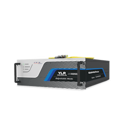
The YLR-AM dual-mode fiber lasers have been developed specifically to eliminate all deficiencies of traditional methods. The YLR-AM laser provides independent rapidly switchable single-mode or multi-mode flat top outputs from a single fiber, allowing users to swap nearly instantaneously between a small spot or larger spots (~3x or ~5x) while independently controlling laser power density on material. Using smaller spot sizes for printing high-resolution features and larger spot sizes for faster build-up rates of the bulk material, YLR-AM lasers provide up to 10 faster printing speeds, several times larger than any alternative on the market. Even higher build rates are possible, depending on material type, part geometry and maximum laser power.
IPG’s solution enables the coaxial emission of either single-mode or a multimode light. The use of single coaxial emission output instead of multiple lasers combined by a complicated external optical setup lowers capital cost, machinery size and simplifies process automation. The faster printing lowers cost per part, reduces capital cost and factory floor area. This solution does not include any mechanical or optical precision components that are sensitive to alignment and vibration and require calibration and maintenance. It is also fully flexible in the amount of power independently provided by the two laser sources.
Meerstetter Engineering GmbH
Laser diode driver LDD-1321 and plug-in TEC Driver PWR-1191
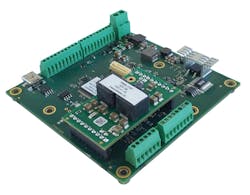
The combination of the low-current CW laser diode driver LDD-1321 (output: 0-1.5 A / 0-14 V) and the plug-in TEC controller PWR-1191 (output: ±4 A / ±20 V) from Meerstetter Engineering offers several significant benefits to designers and systems integrators in various industries. The integration of the LDD-1321 with the PWR-1191 TEC controller provides designers and systems integrators with enhanced precision and control over laser diode operation. By regulating both the current supplied to the laser diode and the temperature at which it operates, this solution ensures optimal performance, constant wavelength, and longevity of the laser diode. The compatibility and seamless integration between the LDD-1321 and the PWR-1191 TEC controller simplify system integration for designers and integrators. They can rely on a cohesive solution from a single manufacturer, reducing compatibility issues and streamlining the development process. Additionally, different interfaces (CANopen, RS485, RS232, USB, etc.) and the free of charge Meerstetter Communication Software simplifies integration into the system as well. The combined solution of the LDD-1321 and the PWR-1191 TEC controller board enhances the reliability and stability of laser-based systems.
The PWR-1191 is based on Meerstetter's longtime development TEC-1091 and promises maximum reliability, accuracy, and reaction speed. The LDD-1321 includes protection features such as overcurrent protection, overvoltage protection, and thermal shutdown (with two inputs for laser diode temperature monitoring). Precise current control and temperature regulation minimize the risk of damage to the laser diode due to overcurrent, overheating, or other environmental factors, ensuring consistent performance over time. The flexibility and versatility of the LDD-1321 and PWR-1191 combination make it suitable for a wide range of applications, including scientific research, industrial manufacturing, medical devices, and telecommunications. Designers and integrators can leverage this solution across various industries, addressing diverse needs and requirements.
The efficient operation of the LDD-1321 and PWR-1191 contributes to increased productivity and cost-effectiveness for designers and integrators. By optimizing power consumption and minimizing downtime due to laser diode failures or performance issues, this solution helps organizations achieve their productivity goals more effectively. The LDD-1321 and PWR-1191 combination leverages advanced features and technologies to provide innovative solutions for laser diode control and temperature management. These include sophisticated PID-control algorithms, real-time monitoring capabilities and look-up-table functions (for arbitrary signal generation), offering users state-of-the-art functionality and performance. Overall, the integration of the LDD-1321 laser diode driver with the PWR-1191 plug-in TEC controller addresses the needs of designers and systems integrators by providing a reliable, efficient, and versatile solution for driving and controlling laser diodes in various applications.
Suzhou Everbright Photonics Co., Ltd
100 W 1710 nm Direct Diode Laser
Everbright is mainly engaged in R&D and production of high-power, high-brightness and high-efficiency semiconductor laser chips. At Everbright, a number of breakthroughs have been made in key technologies such as chip design, MOCVD, lithography, cleavage/coating, package testing, fiber coupling, and so on. The power, brightness, efficiency, and reliability of the laser chip have been greatly improved. Semiconductor laser chips with high power, high brightness, and high efficiency have already put into mass-production, including the 1710 nm laser chips.
The 1710 nm laser chip is proprietary technology of Everbright. The 100 W 1710 nm direct diode laser is manufactured from chip to laser at Everbright, and relevant products like processing heads and temperature control systems are also provided by the company, which means whole solutions can be provided beyond lasers. The 1710 nm laser supported by a welding head and temperature control system can be a solution for outline welding; a rotary welding head and temperature control system can be a solution for spin welding; and a scan system can be a solution for quasi-synchronous welding or mask welding. Due to the high absorption ratio for plastic, the 1710 nm direct diode laser will be a revolutionary product and a big boost to plastic welding, especially in industries like automobile manufacturing, medical instruments, and consumer electronics. Laser plastic welding is much more flexible compared to conventional methods like hot plate plastic welding, ultrasonic plastic welding, etc. No complicated mold is needed, no surface damage is caused, and no scrap is generated during the laser plastic welding process, but lower cost, shorter processing cycle, and better welding quality is earned. Furthermore, the 1710 nm laser is in the vicinity of the peak absorption ratio of transparent plastic. With the unique advantage of a 1710 nm laser, stack welding between transparent plastic materials can be solved. There is also an application prospect in polymer heating.

Peter Fretty | Market Leader, Digital Infrastructure
Peter Fretty began his role as the Market Leader, Digital Infrastructure in September 2024. He also serves as Group Editorial Director for Laser Focus World and Vision Systems Design, and previously served as Editor in Chief of Laser Focus World from October 2021 to June 2023. Prior to that, he was Technology Editor for IndustryWeek for two years.
As a highly experienced journalist, he has regularly covered advances in manufacturing, information technology, and software. He has written thousands of feature articles, cover stories, and white papers for an assortment of trade journals, business publications, and consumer magazines.
