Laser microwelding of copper
The connection of conductive parts for the purpose of electrical contact is one of the oldest, most common joining applications and is required in almost every industry including automotive, electrical and electronic devices, and medical devices. The technologies used to make these connections are driven by cost, joint performance, and volume requirements. As part sizes decrease and performance requirements increase, crimping, soldering, and brazing techniques are becoming obsolete. In contrast, welding, which provides excellent joint integrity, longevity, and conduction performance, is quickly becoming the required standard.
The material of choice is copper due to its ability to efficiently conduct energy and transmit signals. But the very material properties that make copper such a good choice for a conductor unfortunately make it difficult to weld, further magnified with reducing part size, and specifically at a point where we describe the joints as becoming microwelds.
Microwelding of copper presents the significant challenge of controlling the heat balance in these small and highly conductive parts to enable welding but ensuring that over or under heating does not occur. Can a manufacturer satisfy both requirements? Yes—using a 532nm wavelength (green) laser welder.
Before considering the various welding options available, let's define microwelding; the joining of two materials where at least one is less than 0.02 in. thickness. The welding options available are ultrasonic bonding, resistance welding, and laser welding.
Ultrasonic bonding is an effective technique for joining flat copper and other conductive parts; however, as this is a mechanical process, it is limited by the part's resistance to mechanical force, joint access, joint geometry, and different part shape combinations.
Resistance welding is a viable option, but it is subject to access limitations and requires both the purchase and maintenance of small conductive electrodes.
Because ultrasonic bonding and resistance welding both require physical contact with the part to create the joint, the total welding time equals the actuation cycle plus the welding time. For volume manufacturing this adds a significant time delay.
Laser welding, conversely, is a non–contact process, requiring only single–sided access. It is able to access extremely small joint areas and weld different shaped parts. It appears to be a good solution for copper welding—but there is a problem. The reflectivity of copper at the 1064nm wavelength is over 90%. Therefore, to overcome this high initial reflectivity a large amount of power density is required. Once the laser is coupled and the material becomes molten the reflectivity drops significantly. The large power density required for initial material coupling now far exceeds what is required to form the weld. As a result, the material vaporizes leaving a large porosity or a hole.
A number of techniques have been utilized to overcome this reflectivity, including pulse shaping, oxygen assist, and the use of less reflective platings.
Pulse shaping is not reliable as the reflectivity of copper and other conductive parts varies, and so the precise moment at which the laser power should be reduced also varies. There have been some attempts to better anticipate this precise moment by implementing feedback techniques, however none have proven viable. The use of oxygen dramatically increases penetration in seam welding copper by building an oxide layer on the part to be welded, but this has not been effective for spot welding applications because the positive effect of oxygen is seen only after several pulses in succession and thus does not offer a reliable technique for single spot welding or short seams. Using less–reflective coatings such as nickel or tin does help to reduce initial reflection, but does not fully alleviate the problem as large energies are still required to continue the coupling into the copper; thus the process window for microwelding becomes quite small.
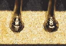
In order to achieve a good, strong laser microweld on copper, one must address the root cause that prevents a good weld: material reflectivity. By reducing the wavelength from 1064nm to 532nm, the reflectivity of copper and other conductive materials is significantly reduced, as shown in the Table. The 532nm wavelength enables consistent laser beam coupling into the copper and stabilizes welding, as highlighted in Figure 1, which shows the comparison of 1064nm and 532nm wavelength welding of uncoated copper. At 532nm the laser beam couples into copper as 1064nm couples into steel.
To microweld copper successfully, a 532nm (green) laser beam is required. This wavelength can be achieved in two ways. Most common is to use a Q–switched laser; however, such a laser does not have sufficient pulse energy to weld. A more novel approach is to use a regular pulsed Nd:YAG laser, which offers 532nm light at 1.5kW peak power with up to a 5ms pulse width. This provides enough weld energy to penetrate around 350–microns–thick copper, which is sufficient for most microwelding applications. Another additional benefit of using a pulsed Nd:YAG laser beam delivered through a fiber is that the beam has low brightness. This promotes even absorption across the focus spot preventing hot spots at the center of the weld that may cause instability.
Applications
Electrical connections come in many different sizes, shapes, and materials. Therefore, a few examples are given to highlight the capability and benefits of using the 532nm welding laser.
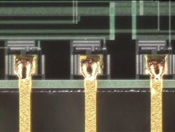
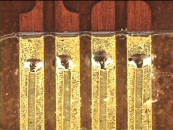
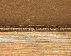
Semiconductor interconnects—The connections shown in Figure 2 are 0.0015in.–thick gold–coated copper flat wire bonded to metallized pads. As the wire was wide but very thin, a relatively large spot size was required to make the weld. A long pulse width with low peak power enabled good flow within the bond, and the low brightness of the beam enables uniform heating across the width of the flat wire.Dissimilar materials—When welding materials with different levels of absorption, there is a tendency to overheat the more absorptive materials causing excessive spatter and porosity. This is usually overcome by favoring one material, however for small parts this may not be sufficient as even the tiniest absorption imbalance can create an overheated weld. At 532nm wavelength the reflection of both parts becomes closer, therefore the weld energy balance is more consistent, significantly improving weldability (see Figure 6).
Summary
Welding copper is a difficult proposition; microwelding copper presents an even greater challenge. Laser welding offers a useful method for joining, offering a non–contact process well geared for automation. However the reflectivity of copper at the 1064nm wavelength has always been the barrier to implementing laser welding. By using a 532nm green Nd:YAG laser welder this barrier has been removed, offering a viable method for microwelding copper and other conductive materials in high volume.
Geoff Shannon, Ph.D. | Director Strategic Marketing for Precision Manufacturing, Coherent
Geoff Shannon, Ph.D., is Director Strategic Marketing for Precision Manufacturing at Coherent (Santa Clara, CA) and an Editorial Advisor to Industrial Laser Solutions. He previously served as Laser Technology Manager for Miyachi Unitek, specializing in the development of lasers and applications for existing and new markets. Shannon has a BEng in Mechanical Engineering and PhD in Laser Welding Technology from the University of Liverpool. His 20-year career in laser technology has centered around applications research and development and new product development of lasers and systems.
Paul Severloh | Sr. Laser Welding Applications Engineer/Process Development Engineer, Amada Miyachi America
Paul Severloh is Sr. Laser Welding Applications Engineer/Process Development Engineer at Amada Miyachi America (Monrovia, CA).


