Lasers fit the bill for the ever-shrinking requirements of manufacturing
Greg Anderson
The image of sparks flying and the precision of large-scale five-axes laser systems have become familiar icons in the industrial world, with equipment makers represented at major tool shows such as IMTS, held in Chicago every two years. A new series of laser tools have begun sharing the limelight recently-laser micromachining systems.
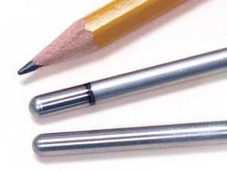
Example of thin-wall (0.010-inch) stainless-steel welding and then polishing of tube and end cap.
These laser products provide a technology road to the advanced requirements of today’s industrial manufacturing with ultra-precision and an almost infinitely small tool size. The ever-shrinking requirements of manufacturing are a reality whether you are trying to fit billions of electrical instructions on a chip the size of a quarter or producing a gear and rack the size of a human hair.
Laser micromachining technology provides solutions to problems that, perhaps, cannot be solved other ways. For example, it enables machining with no part contact and no mechanical force applied to the part, and it offers the ability to provide an almost infinitely small tool bit that cannot break. The availability of different laser wavelengths can be targeted to process certain materials but ignore others on the same part. The energy control and output consistency of lasers can produce depth control in microns. Material hardness is not a significant issue for laser processing, so that drilling a 0.005-in. diameter hole in ceramic or diamond is the same as stainless steel, copper, or FR4 PCB material. Because of the small laser beam spot size and controlled energy, laser welding of delicate parts such as foils, thin featured items, or hermetically tight welds are not a problem, so that extremely small holes, even blind holes, are readily done with the right wavelength and optics.
One of the most useful characteristics of laser technology is the wavelength of the laser beam. Laser wavelengths come in every color, visible and invisible. All materials absorb or reflect different wavelengths of light; silicon, used in the manufacture of IC dies-the brains of an IC chip-typically do not absorb light above 1100 nm. Glass, silica, or most materials that are clear will transmit the IR wavelength at 1064 nm allowing the beam to pass through this material with no affect. The CO2 laser, at a wavelength of 10,600 nm, is absorbed by most organic materials regardless of their color.
These characteristics are routinely utilized by laser micromachining systems to uniquely do their jobs. For example, a back-lit button seen on a car radio comprises a plastic button with a layer of white paint, followed by a layer of black or another dark color. An IR (1064nm) wavelength laser removes the black paint, which is absorbed by the laser, but is reflected by the white paint with the top layer being removed without damaging the white layer beneath. Add a little light and you have the “glow in the dark” radio buttons.
When you have a series of multi-colored packaging labels that need a “born on date” and lot number for a required permanently marked identification, a CO2 (10,600nm) wavelength laser is used whose beam is absorbed by all paints or inks whether they are white or black.
Another problem is how to hermetically seal weld a stainless-steel implantable pacemaker that must be welded in a vacuum? Using a vacuum glovebox that utilizes a set of internal gloves to load and handle the part, a glass window is inserted in the top of the device, then using an IR (1064nm) laser, with a beam that transmits through glass, a weld is made on the part inside the vacuum chamber.
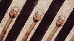
Example of wavelength-selectable processing. 1064nm laser ablates mold compound but preserves tiny bond wires and bond pads-IC failure analysis
Lasers are available as high-frequency, continuous-charged laser cavities with Q-switched pulse frequencies from 1 KHz to 100 KHz (some pulsed lasers even as high as the MHz range) and lower-frequency pulsed laser designs in the range of 10 Hz to 100 Hz. The lower the Q-switch frequency the more off time there is and power in each pulse is greater. This lower frequency is used for cutting, drilling, and machining. Higher frequencies with less peak power per pulse but greater average power are used for welding, melting, and cuts or scribes that are not affected negatively by heat affected zones (HAZ).
In pulsed lasers, each time the laser is pulsed a single burst of laser energy is emitted. These pulses are generally of a much greater energy level than a Q-switch laser and the control of the energy is better. A pulsed laser with its extremely consistent pulse energy is used in many situations where precise depth control is demanded or for drilling deep holes in difficult materials.
The pulsewidth of a laser is inherent in the design of the laser cavity and is probably one of the most important attributes used in micromachining. At each pulse of a laser, whether it is a Q-switched laser running at between 1 KHz and 100 KHz or a pulsed laser operating between 1Hz and 100 Hz, there is duration of time that the actual energy of the pulse is released, usually measured in nanoseconds. This time interval is crucial to any process attempted by the laser system. If the pulsewidth is short, less than 60 nanoseconds, a process of ablation or vaporization of the target material takes place with very little HAZ. Many critical machining tasks may be done with no heat affect on areas or components close to the lased path. Laser cuts may be made on live electrical devices with no changes in electrical characteristics except those that were intended.
Example of pulsewidth and HAZ affects - 15-micron holes in ceramic. The left hole was done with a picosecond UV laser and the right hole with a femtosecond UV laser.
Longer pulsewidths, above 100 ns, have much less peak power per pulse but because the energy is there longer these pulses can provide processing features useful in a host of laser applications. When a material is too sensitive to tolerate the shock of the higher energy of a shorter pulsewidth, such as diamond drilling or cutting, or needs the greater heat or laser absorption to provide a cleaner edge quality in cutting or scribing, such as is required in ITO trimming, the longer pulsewidth is an asset not a detriment.
One obvious asset of a laser beam is that no matter how small (even less than 25 microns) it never breaks off in the workpiece and it never gets dull in the middle of machining a part. This trait of non-contact processing has myriad advantages.
No torque is applied to the part so fixturing can be minimal and inexpensive. Many systems use no fixturing at all: a part is placed under a vision system, the location and angle are established and are sent to the lasing computer, and the part is processed. Other systems allow the operator to lay a part under a camera and then a CAD image is “dragged and dropped” to the correct location and the part is machined.
This idea of an infinitely small tool bit is desirable because in traditional machining, and especially micromachining, the smaller the tool the more difficult the associated problems. Conventional tools break, small drills bend or walk out of position, and end mills or even EDM electrodes are only practical to a certain minimum feature size.
By changing wavelengths and optics the laser spot size can be manipulated to achieve almost any size requirements. Kerf widths as small as 25 microns, hole sizes as small as 25 microns, and, through the use of masks and image plane optics, features in the micron and even sub-micron range are possible.
Many micromachining applications involve precise depth control to micron and sub-micron accuracies such as in a lubrication film pocket or a trench machined in flexible materials for a fluid circuit device.
Other examples may require removing a layer of material to micron tolerances to protect underlying components as in the case of cutting a copper layer in a miniature multi-layered hybrid circuit board without damaging other layers below. Another example is the removal of the outer insulation layer of a multi-conductor cable without affecting the insulation of the inner wire when the entire cable is only 200 microns in diameter and the thickness of the insulation is in microns.
Materials that are too hard to be machined with most conventional methods are prime candidates for laser micromachining. Diamonds for example are used in many places in the industrial world as well as in jewelry and cosmetics. And laser technology is used in the manufacture of water jet nozzles and the production of dies used for wire drawing. For the nozzles used in abrasive water jet systems, a small hole or orifice is laser drilled in a diamond insert. These nozzles are subjected to pressures in excess of 55,000 psi with water flows of 3000 ft/s. The holes range from 50 to 400 microns in diameter.
To produce very small wires, material is drawn through the wire die; it is obvious why diamond is the material of choice in these circumstances.
The idea of drilling extremely small or deep holes in tough materials such as Hastalloy to produce cooling holes in jet engine blades is yet another example of a manufacturing process that relies on laser technology. In this application a pulsed laser is used in a percussion drilling mode. This technique utilizes a repeating pattern of pulses where each pulse of consistent high energy removes a fixed amount of material.
The small spot size and controlled, consistent energy of the laser microwelding system renders it ideal for welding in situations that are not practical with conventional MIG, TIG, gas, or wire feed devices.
A thin-walled, 1.8mm diameter, electronic crystal can with a wall thickness of 125 microns and the internal component cover need to be welded together with the lid located approximately half way down inside the can. The only way to join this component without excess heat is with a focused laser beam.
The uses of laser micromachining systems in today’s high-technology world of manufacturing and even in many of the low-tech traditional productions are endless. The basic characteristics of laser technology and the examples mentioned here barely scratch the surface of this rapidly evolving manufacturing tool.
Greg Anderson is president of Control Systemation Inc. (CSI), providers of laser micromachining systems, Orlando, FL, www.controlsystemation.com.


