While the use of lasers to scribe materials is not new, the application of this process to dice semiconductor chips has been more difficult to implement because of the sensitive electronic nature of the final product. This difficulty is even more acute in devices fabricated on such a hard substrate material as sapphire for the burgeoning gallium nitride (GaN) light-emitting diode (LED) and semiconductor-on-insulator (SOI) industries. However, over the past six years the cost per pulse for ultraviolet lasers has decreased rapidly and advances in process integration have allowed for this method to become not only viable but also preferred.
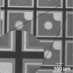
There are several traditional methods for separating these wafers with arrays of die into individual chips, including dicing saw separation and scribe-and-break, but they can waste valuable wafer area, involve costly consumables, and have long process times. More recently, a technique called laser scribing, which overcomes many of the difficulties associated with the older technologies, has been developed. A given die should have a uniform size, a consistent shape, no visual defects, the desired performance, and excellent reliability, all performed at a low cost. The process sequence for laser scribing to achieve all of these characteristics involves the following steps: preparing the surface with a protective coating, mounting the wafer on a tape backing, scribing the wafer with the laser, fracturing the wafer with a mechanical roller, and cleaning the protective coating. The protection and cleaning process allows for the scribe lines to come within a few microns of active features on the die (see Figure 1 inset).
Figure 1. An example of a clean, diced sample LED wafer with a narrow kerf width with the inset detailing how closely the scribe lines can get to active device area without damage.
Most devices with sapphire substrates employ metal and topographic features, often close to the edge of the chip, which must not be damaged during separation. Saw separation uses a blade with embedded diamonds to remove the material via a brute force approach. This technique is generally not used for sapphire, except for large die or wafers, because it requires wide streets (with a kerf width up to 250µm) and wastes a lot of active wafer area. The scribe-and-break technique mechanically weakens the substrate by employing a diamond scribe to provide a fracture line between die. A sharp straight edge then breaks these rows. This results in a narrow kerf width, but the wafers must be thinned below 100µm to achieve consistent yields above 80 percent. A polishing step may also be necessary to reduce strain caused by the device layers on top of thinned sapphire. These two processes have been effective on silicon and other III-V substrates because the material is much softer than the diamond, however there have always been tradeoffs with sapphire.
Laser scribing offers many advantages in a manufacturing setting. The combination of a narrow kerf width, high throughput, and wide process tolerance results in a more robust process flow at lower cost. The most time consuming and costly step in dicing, and the one that causes most yield problems, is precise control of the sapphire thickness. Saw separation does not generally employ thinning, however chip-outs as well as blade wear and breakage are frequent. For scribe-and-break to work, it must maintain a tightly controlled thinning process, and in the case of LEDs, there is a performance benefit as a thicker chip aids in light extraction. With laser scribing, yields between 97 and 99 percent with a wafer thickness up to 700 µm may be achieved because the cut depth can be adjusted easily while maintaining the same kerf width. One other novel feature of the laser scribing process is the ability to scribe both the front and back of a wafer before fracturing to provide a more uniform die shape, especially useful for LEDs because of the requirement for uniform light emission. It is much more difficult, if not impossible, to flip a wafer over after the saw or scribe-and-break process and maintain high yields.
Compared with the other techniques, laser scribing has a 5 to 20 times faster throughput because the laser beam can be projected on the wafer surface as a long line or multiple lines, which are scribed simultaneously. With the accompanying process steps factored in, this typically increases the process throughput by a factor of 3 to 10 times for LDS compared to other techniques. The laser scribing process throughput increases as the energy of the laser and length of the beam (or multiple beams) increase.
The main trade-off in determining the proper laser for scribing is the desired throughput versus cost. The throughput is based on the wattage of the laser power and the efficiency of the optical system. The absorption properties of GaN for LEDs, which is transparent below 365nm, and sapphire (semi-transparent between 177 nm and 9.5 µm), are important in selecting the proper laser for a given material. The laser should be fast enough to produce a small heat-affected zone and cut through the thin device layers by melting and the sapphire via laser ablation, thus preventing damage to the active device area. The choice of laser for this process is thus optimized between 177 nm and 365 nm with pulses less than 30ns. The two most likely choices are the KrF excimer gas laser operating at 248nm and the frequency-quadrupled Nd:YAG diode-pumped solid-state (DPSS) laser operating at 266 nm. Nd:YAG lasers operating in frequency-tripled mode are more powerful operating at 355nm, but for LED applications the proximity of the absorption band of GaN causes some device degradation. The DPSS laser can achieve slightly smaller kerf widths than the excimer laser (5 µm versus 15 µm) with reduced laser maintenance.
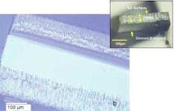
Regardless of the laser, scribed lines are clean and precise (see Figure 1), which also helps manufacturing by aiding in visual inspection. The desired scribe depth is usually 55 percent of the total thickness and decreases for thinner sapphire substrates. An image of the sidewall of a die cut with the laser is shown in Figure 2a. The double-sided scribing process also affords more process tolerance because scribe depth can be checked in the middle of the process (see Figure 2b).
The use of this laser scribing technology has truly become cost competitive with traditional die separation techniques. The advantages of high throughput, low cost, ease of use, process tolerance, and high yields means that this technology has become the preferred choice and will continue to be adopted by the semiconductor industry over the coming years.
Bryan S. Shelton, Ph.D., is the manager of electronic device development at Emcore Corporation (Somerset, NJ). He acknowledges the contributions of Mark Gottfried, Michael Sackrison, Tony DiCarlo, and Ivan Eliashevich.

