Lasers play an important role -from microfabrication to nanoprocessing-in next generation manufacturing
Minghui Hong
Precision engineering is shaping our lifestyle as an important manufacturing pillar. As a vivid example, the hard disk for information storage was first introduced by IBM in 1956. RAMAC 305 (capacity ~4.4 MB, stored in fifty 24-in disks) was leased for $3200 per month in 1957 dollars, equivalent to a purchase price of ~$160,000. Today we can easily buy a 1-in 5Gbytes Seagate disk drive at ~$100. Over 50 years, the disk drive price per Mbytes dropped about 2 million times while its recording density increased ~100 million times. As a result, personal computing moved from a huge hall into our home or onto a laptop. We can download thousands of songs, put them into iPod devices, and enjoy the music as we move. We can store street landscape information for 3D car navigation so that driving in a strange place is no longer a difficult task. We can set up video-on-demand systems for non-stop entertainment by zipping huge video programs into small data storage plates. All of these capabilities can be attributed to advanced precision engineering techniques, which are able to fabricate functional micro/nanostructures at a low cost. The laser provides unique advantages over other precision engineering tools, playing an important role in manufacturing with much more extensive applications.
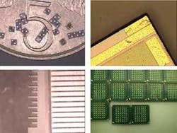
FIGURE 1. Laser singulation of GaAs, Si thin wafers, glass substrate, and CSBG IC packages.
Laser singulation
Wafer singulation is a key process in microelectronics production lines, where it is used to separate thousands of IC dies from an 8- or 12-in wafer in a market of about $20 billion. Driven by the demand for smart cards, implantable medical devices, security/keyless entry systems, portable computing, and military and aerospace applications, the wafer industry is moving toward the mass production of large memories for mobile phones, cell base stations, PDAs, Internet routers, and on ever-thinner substrates for 3D packaging. This movement leads to extreme technical difficulties for current diamond saw dicing, which makes thin wafers chip and crack and causes device failure as the fast rotating metal plate runs over wafer streets. Meanwhile, it is also facing technical challenges in separating difficult processed substrates, such as glass, sapphire, diamond brittle substrates, and glass/Si/glass multi-layer device structures.
Pulsed laser ablation is a process for fast and explosive removal of substrate materials by tightly focusing a laser beam down to a few microns diameter. The heat affected zone (HAZ) can be limited to dozens of microns due to short pulse duration and small light absorption depth. With novel processing approaches such as steam laser ablation and pocket scanning, pulsed laser irradiation has achieved high-quality singulation of thin GaAs and Si wafers (50 and 100 μm) at a speed up to 100 mm/s and a singulation street of 20 μm wide. It is also used to achieve high-quality microcutting of glass substrates with finely defined corners and multi-layer structures of chip scale ball grid (CSBG) array packages with uniform cross sections. Figure 1 shows the singulation results by 355- and 532nm DPSS Nd:YAG lasers, which are technically mature and cost-effective for these industries.
Laser disk tagging
For product control in data storage industries, tracking of products throughout the whole life cycle is an essential requirement in hard disk fabrication. An important cost-effective measure in production uses one side of the disk even though the other side does not pass critical testing. A long-time engineering problem for hard disk manufacturers is how to code serial numbers and characters on super smooth and clean magnetic media disks. The technical challenge comes from the critical requirement of ultra-low flying height, about 10 nm for high recording density. New processes should fit into high-class cleanroom manufacturing environments. Conventional laser marking processes are based on the removal of the substrate materials to create contrast, but this introduces contamination into the production environment. Laser disk tagging is a novel process to create contrast based on different heat absorption and dissipation during laser irradiation of the multi-layer thin film structures. This new technique has been successfully commercialized and dozens of laser disk tagging machines are currently running in hard disk media production lines. With new processing designs, this novel laser marking can find more extensive applications in non-contamination marking of other substrate devices.
Fs laser perforation
Pulsed laser ablation is a unique technique that fabricates tiny structures on substrate surfaces for bio-medical applications. Polycaprolactone (PCL) membrane is a biodegradable polymer, which can be absorbed by human bodies after a couple of weeks’ implantation. In order to develop new tissue engineering applications, it is bi-axially stretched down to a few microns thickness. Chemical treatment and needle perforation are two conventional methods to improve its wettability for bio-molecule/cell attachment. However, the first method deteriorates bulk thin film quality with chemicals involved while needle perforation can not completely punch through the hole with polymer flaps tending to close when placed in a cultured solution.
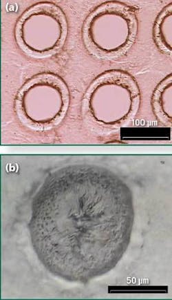
FIGURE 2. (a) PCL membrane and (b) blind hole fabricated by femtosecond laser perforation.
A femtosecond laser was used to drill tiny through-hole arrays and fabricate the PCL membranes. The ultra-short pulse duration laser irradiation can either eliminate heat or control the applied heat to a minimum on thin polymer films. Laser processed PCL membranes possess excellent hydrophilic properties to anchor bio-molecules during the cell culturing. With flexible CNC programming, different geometric designs of laser processing contours can be created for special tissue engineering requirements. Further, blind-hole array fabrication by laser perforation and welding also provides a novel approach to make tiny nanomedicine powder capsules. Their size can be as small as a few microns. With proper drug delivery mechanisms, these small gadgets can be transported to the targeted positions to cure the diseases. As the biodegradable PCL thin films-the outside of the capsules-are absorbed, the nanomedicine powers are released on the spot. This would be beneficial for patients in curing diseases with smaller side effects and greater efficiency. Figure 2 shows the PCL membrane and blind-hole fabricated by the fs laser perforation.
Technical developments
There is an ever-increasing demand from industries to fabricate smaller, faster, and more functional micro/nanodevices; nanoengineering technology may be inevitable to push device feature size down to 100 nm. Compared to electron beam and focused ion beam processing, laser nanoprocessing has the advantages of low cost, high speed processing in air, vacuum, or chemical environments, and most importantly it has the capability to fulfill flexible integration control into production lines. How to break through optical diffraction limits with mature, stable ultraviolet (UV) or visible light sources is attracting research interests around the world. Following are a few laser nanoprocessing approaches, which are being developed to fabricate nanostructures in our laboratory.
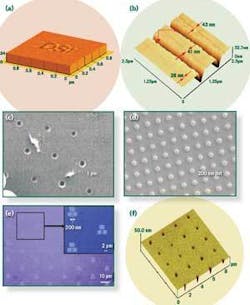
(1)-A 532nm/7ns Nd:YAG laser beam was introduced into a gap between a scanning probe microscopy (SPM) tip and substrate surface. With the tip scanning over the surface, 10nm resolution nanolines and nanocharacters were fabricated on metal and photoresist surfaces. Depth and width of the nanolines depends on many factors, such as tip sharpness, scanning speed/time, and laser fluence. The mechanism of laser/SPM surface nanopatterning is quite complicated. During the laser irradiation, the SPM tip and substrate surface absorb laser energy and induce the thermal expansion to process the substrate surface. The other possible mechanism is during the laser irradiation, the tip functions as an antenna. It enhances the electric field under the tip so as to etch away surface materials to form the nanopatterns. Figure 3(a) shows an AFM image of 400nm × 400nm “DSI” characters written on a thin film surface.
FIGURE 3. Surface nanostructures fabricated by (a) laser/AFM, (b) femtosecond laser/NSOM integration, (c) laser/transparent nanoparticles, (d) laser interference lithography, and (e) and (f) laser nano-imprinting.
(2)-A 400nm/100fs laser was applied to irradiate thin photoresist-coated substrates through a near-field scanning optical microscopy (NSOM) fiber tip for surface nanopatterning. Aperture size of the NSOM is ~50 nm. The tip/sample distance was regulated at dozens of nanometers by a tuning-fork-based shear-force detection feedback. The laser beam coming out of the NSOM tip is in the form of evanescent wave, which decays quickly with increasing distance but contributes significantly to the sample process in near field. At small aperture size and probe-to-substrate distance, the NSOM overcomes the traditional far-field diffraction limit to create sub-wavelength-size patterns. Figure 3(b) shows the nanoline arrays created at different incident laser powers. With the fine tuning of laser power and writing speed, nanoline arrays with the linewidths of 20 ± 5 nm were created by fs laser/NSOM integration. Such high resolution can be comparable with electron beam lithography for new functional nanodevice fabrication. Furthermore, these small nanopatterns were fabricated in air with only the light irradiation in near field. It is not affected by electromagnetic wave interference, which worsens the electron beam lithography resolution. With a multi-NSOM fiber tip design, parallel nanolithography can be fulfilled for high-speed surface nanostructuring by the fs laser/NSOM integration.
(3)-Sub-100nm nanostructures were created on substrate surfaces with pulsed laser irradiation through 1mm transparent particles self-assembled as a mask, due to laser light intensity enhancement near the contact area between particle and substrate. Because the distance between particle and substrate is much smaller than light wavelength λ and particle size is smaller or in the order of λ, laser irradiation of the particles on the substrate is different from the situation of a spherical lens focusing in the far field. It is the optical resonance effect in the near field. Mie theory simulation shows that for 266nm laser and 500nm particle, light intensity is enhanced up to 50 times at the particle center. Besides the laser processing parameters, nanopattern sizes are also dependent on particle diameter and λ. Figure 3(c) shows nanohole arrays created with laser irradiation through transparent particles approach.
(4)-The principle of laser interference lithography for high speed and large area period nanostructure fabrication is based on the interference of coherent light to form a horizontal standing wave pattern in far field, which can be recorded on photoresist. For two beam interference, the standing wave forms a grating pattern with a few minutes of laser light exposure. The period is dependent on light wavelength and the intersect angle of two incident beams. The size of the grating is determined by the laser coherent length. By a 90° sample rotation and the second exposure, a grid pattern on resist can be defined. After chemical etching and a lift-off process, the nanostructures can be transferred onto the substrate for many potential applications, such as patterned media in high density data storage, microsieves for micro-filtration and sub-micron perforated membrane, templates for self-assembly and field emission flat panel display. Figure 3(d) shows an SEM image of the nanostructures fabricated by the laser interference lithography technique.
(5)-Laser nano-imprinting is a non-contact, multi-beam, maskless nanolithography approach. Sub-50nm feature size was achieved by laser combination with AFM, NSOM, and transparent particles. The processing speed is quite slow (in μm/s scale), which limits their applications in industry. Laser nano-imprinting by light irradiation through a microlens array (MLA) was explored. Microlenses can convert the laser beam into thousands of small focal points, which act as an array of “light pens” (multi-beams) to fabricate tiny structures uniformly over a large area at a high speed. This is a non-contact parallel laser imprinting process in far field as the MLA is dozens of microns above the substrate. Figure 3(e) is the optical image of field emission transistor (FET) structures fabricated on GeSbTe thin film by 800nm/100fs laser irradiation through a 23µm diameter MLA. CNC programming controlled nanostage moved the substrate during the laser irradiation. It is maskless nanoprocessing, which can save hundreds of thousands of dollars in photomask fabrication. The inset is the enlarged image of the features. It shows that 160,000 FETs with the gate width of 200 nm can be created in three minutes on an area of 1cm x 1cm. With smaller MLA patterning, sub-80nm dot arrays, as shown in Figure 3(f), were created on the substrate surfaces with a single pulse of 248nm/30ns KrF excimer laser irradiation. Compared with other nanoprocessing techniques, laser nano-imprinting would have much higher potential to be adapted by industry for large-area and high-speed nanomanufacturing in the near future because it is a non-contact, multi-beam, maskless process.
Dr. Minghui Hong ([email protected]) is with the Data Storage Institute, Agency for Science, Technology and Research, Singapore Department of Electrical & Computer Engineering, National University of Singapore, Singapore.

