Pulsed nanosecond fiber lasers can join dissimilar materials
Industrial use of nanosecond lasers for applications such as marking, engraving, cutting, and even micromachining is well known—however, the use of these sources for welding and joining is relatively new [1]. Most applications of high-peak-power, short-pulsed lasers tend to be related to material removal, so their use as a beam source for joining is perhaps counterintuitive. But for those in the know, the versatility afforded by master oscillator power amplifier (MOPA)-based nanosecond fiber sources give unparalleled flexibility in terms of control of the output characteristics. These lasers can be used, for example, with high-peak-power nanosecond pulsed output with tunable pulse duration and high frequency-modulated quasi-continuous-wave (QCW) modes, as well as operated as a more conventional continuous-wave (CW) laser.
On paper, one could quite rightly question the capability of these lasers for welding. Compared to CW and QCW sources, they have very low average powers (typically <100W) and pulse energies of just 1mJ, which is 1000X less than typical diode-pumped solid-state (DPSS) and QCW pulses. This does currently restrict the use of pulsed fiber lasers to relatively thin sections up to 0.5mm, but recent results show that penetration depths of up to 1mm are possible. Operating with pulse durations often in the 100–500ns range, with peak powers of up to 10kW and pulse repetition frequencies of >50kHz, these lasers are significantly differentiated from conventional QCW sources. This ability to tailor the input energy characteristics to the application at hand is key to their use as a tool for joining.
In general, when bonding thin material, there is a requirement for reliable joining processes that avoid over-penetration, distortion, and warping. This is addressed by conventional keyhole welding processes using CW lasers, but overcoming material thresholds requires relatively high powers (usually >200W). The challenge is even greater for joining bright metals, and even more so when the materials are dissimilar.
Challenging convention
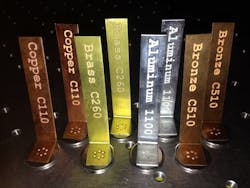
The joining of dissimilar metals has long been a challenge for welding and design engineers who have often been told that it's difficult or that it can't be done. Every welding handbook contains a table showing the allowable combinations of materials that can be welded—and those that can't. As any metallurgist will tell you, it is the combination of physical properties and metallurgical incompatibility that governs weldability. However, there has always been a lot of interest in this area because there are a lot of potential applications that require such joints, particularly bright metals to steels and aluminum alloys. Over the years, this has prompted a significant research focus in this area—innovation has been incremental, so it's still work in progress. SPI Lasers' nanosecond welding process (patent pending) has provided a differentiated mechanism that has to date proven itself to be extremely capable in joining a wide variety of dissimilar metals (FIGURE 1).
Fusion welding of dissimilar metals creates problems associated with the formation of brittle intermetallic phases. These can form planes of weakness, making the joints susceptible to fracture. These intermetallics typically manifest themselves in the interface of the weld pool and form based on time and temperature. Heat input is a key factor in their formation.
The use of nanosecond lasers for joining is unlike conventional welding in that it does not generate a large melt pool, so opportunity for the formation of these unwanted intermetallic phases is inhibited. The spot size is very small (often in the 30μm range), so to make spot welds or linear welds, techniques such as spiraling and beam wobbling are used. The spot size can be easily changed by appropriate selection of beam expanding collimators. The majority of the processing was conducted with our 70W EP-Z lasers with an M2 of <1.6. However, for some applications, it has been found that a broader energy distribution, as offered by the 70W HS-H model with its M2 of 3.0, results in improved joint characteristics.
The joining of copper to aluminum (with the copper on top) is a joint of significant commercial interest. It is technically challenging in that the copper is highly reflective and conductive, presenting the laser with a high threshold to enable coupling of the incident laser beam and the subsequent initiation of the weld. The high peak power of the nanosecond pulses is crucial to overcoming this threshold and aids coupling into the material. It does such a good job that the resulting joint is somewhat unusual. The cross-section through a weld made through copper into aluminum shows the kind of microstructural features that can be achieved (FIGURE 2). It can be seen that the beam penetrates through the upper layer of copper and melts the aluminum below. There is incomplete mixing and the aluminum is absorbed through the copper to form more of a metallic bond between the two layers, resembling a rivet.Harnessing power
A major area of current interest is the welding of battery cells, where the key challenge is to join multiple cells. A wide range of materials are being studied, including aluminum, copper, and nickel-plated copper. The objective is to produce a reliable and tolerant process that generates strong welds with no burn-through or witness mark on the battery contact. Heat input into the part can be critical and this can be accurately controlled by nanosecond welding. The material thickness of the tabs tends to be in the 250–500μm range, which is generally within the capability of the nanosecond joining process range.
The nanosecond welding process offers multiple options in the join design-for example, it is possible to produce a single large spot or multi-spot arrays. Studies have shown that although the contact area per given welding time was roughly the same, multi-spot arrays have proven to be stronger (both in tensile and peel strength) and give greater control of heat input. Using a 3 × 3 array made in approximately 2s using a 100W laser, it can be seen that no burn-through or witness mark is made on the underside of the battery cap. Peel testing has shown these joints to be incredibly strong and that the failure occurs in the heat-affected zone (HAZ) adjacent to the weld nuggets, leaving the weld stubs intact. FIGURE 5 shows welding of nickel-plated copper and aluminum tabs to standard lithium-ion cells.Weld geometry flexibility offered by the nanosecond welding process through use of scanner-based beam delivery opens up many possibilities to design joint configurations that are fit for purpose. Whether it's for electrical conductivity, pull or peel strength, penetration and nugget shape, utilizing available space, or minimizing heat input (no witness mark welding), the weld shape can be optimized.
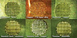
An example of an interesting join option is the use of grid patterns, which can be done at extremely high speeds to cover available areas. This has been shown to be extremely effective in joining a wide range of dissimilar metals, including copper on 718 super alloy, aluminum on brass, aluminum on copper, stainless steel on aluminum, stainless steel on copper, titanium on aluminum, and titanium on copper. In fact, we struggle to find material combinations that we have not managed to join with some degree of success (FIGURE 6).Working for a stronger future
The engineering and design community is showing strong interest in welding thin dissimilar metals across a broad range of industries, including consumer electronics, semiconductors, batteries, sensors, and medical, to name just a few. Our testing has shown that most combinations of widely used metals can be joined using the nanosecond welding process to give an acceptable joint strength for numerous applications and industries. Of course, there is still a great deal of work to be done to categorize the various material combinations and to more fully understand the process fundamentals, but what is certain is that this opens up new opportunities for today's manufacturing design engineers. Nanosecond lasers will open up an exciting new dimension to joining of both similar and dissimilar metals.
REFERENCE
[1] J. Gabzdyl and D. Capostagno, "Pulsed nanosecond fiber lasers can weld, too!" Industrial Laser Solutions, 30, 5, 21–25 (Sept/Oct. 2015).
About the Author
Jack Gabzdyl
Industry Manager – Electronics, TRUMPF Laser UK Ltd
Dr. Jack Gabzdyl is Industry Manager – Electronics at TRUMPF Laser UK Ltd (Southampton, England) and has more than 30 years of laser materials processing experience. He obtained his PhD in laser processing from Imperial College London in 1989. He has since had a number of technical and marketing positions at BOC Gases, Advanced Laser Solutions, and TWI before joining TRUMPF (formerly SPI Lasers) in 2007.
Daniel Capostagno
Applications Manager - Americas, SPI Lasers
Daniel Capostagno is Applications Manager – Americas at SPI Lasers, Santa Clara, CA.


