Excimer laser annealing allows production at high volume
RAINER PÄTZEL and RALPH DELMDAHL
Using polycrystalline silicon (poly-Si) as a thin-film transistor material enables the fabrication of flat-panel displays with improved appearance, higher speed, and lower power consumption. Because of these advantages, the use of poly-Si transistors is becoming increasingly popular for mobile device displays. The method of choice for producing these displays is excimer laser low-temperature polycrystalline silicon (LTPS) annealing—this article reviews the basics of LTPS and how it is currently being implemented in display production.
Flat-panel basics
The two most common technologies currently in use for flat-panel displays are active matrix liquid-crystal displays (AMLCDs) and active-matrix organic light-emitting diode (AMOLED) displays. Both of these display types utilize a backplane consisting of a glass substrate on which a large number of thin-film transistors (TFTs) are created to form the actual pixel circuitry. The thin film is made of silicon (typically 50nm thick), which is patterned using traditional integrated circuit (IC) fabrication methods to yield the desired circuit structures.
Solid silicon can take on three different forms at room temperature, namely poly-Si, amorphous (a-Si), and single crystal. As the name indicates, in the single-crystal form, all the atoms are in one large, continuous lattice. This configuration delivers the highest electron mobility (~600cm2/Vs) and conductivity, and is the form used in all types of integrated circuits. The atomic arrangement in amorphous silicon is highly irregular and disordered, resulting in significantly lower electron mobility (~0.5cm2/Vs). The poly-Si form is intermediate between these two extremes, with the atoms forming microcrystals or grains, and having discontinuities between these grains. This yields electronic properties that are between (electron mobility of ~50-250 cm2/Vs) the extremes of the other two forms.
The silicon substrates used for ICs are created through epitaxial growth to yield a virtually defect-free, single-crystal silicon boule. This boule is then physically cut to produce individual wafers for subsequent circuit fabrication. This method isn't applicable to flat-panel display applications-rather, the silicon layer is deposited onto the glass using low-pressure or plasma-enhanced chemical vapor deposition (LP-CVD or PE-CVD). Either method results in a suitable layer of a-Si on the glass substrate.
Unfortunately, the poor electron mobility in a-Si yields several significant limitations in both AMLCD and AMOLED displays. These can be solved by the use of poly-Si in the backplane. In the case of AMLCDs, the use of poly-Si improves circuit electrical efficiency, which enables the use of TFTs with reduced area and narrower circuit traces. In turn, these smaller circuit components block less of the backlight, allowing the display to appear brighter while simultaneously drawing less power. Physically smaller pixels are particularly critical in current smartphones to support the small, high-resolution displays that require pixel densities in the 400-900 pixels/in. range because of the close viewing distance.
AMOLED displays don't incorporate backlights because the pixels themselves emit light. But stable, low-impedance control circuitry is critical for these displays because each pixel draws current, making electron mobility and TFT current stability even more important. As a result, poly-Si is the requisite form, and it is currently in use for all small- to medium-sized AMOLED displays.
Poly-Si annealing
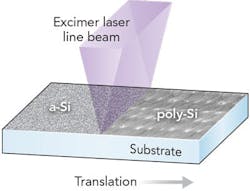
The a-Si created through vapor deposition can be transformed into poly-Si by thermal annealing-that is, heating it until it melts and then cooling it. The most obvious means of accomplishing this would be to simply heat up the entire glass panel. However, the required temperature for this process is 600°C. This high temperature would damage standard glass substrates, and therefore necessitates the use of expensive, heat-resistant substrates. This high-temperature process was employed in production when flat-panel displays first became popular. But as panel sizes increased, the display industry sought an alternative approach that could be performed at lower temperatures, and would therefore eliminate the use of expensive quartz or thermal glass substrates. The alternative method that emerged was LTPS annealing (FIGURE 1).
In this technique, a pulsed excimer laser line beam is scanned over the a-Si film. Silicon efficiently absorbs the 308nm excimer output. This high absorption, combined with the high pulse energy of the excimer laser, makes it possible to achieve near-complete melt of the thin silicon layer with just a few pulses. This near-complete melt is essential to achieve the optimum crystal formation (in terms of resultant electronic characteristics). The high absorption of the silicon also prevents the UV light from penetrating significantly into the glass substrate below, thus avoiding any consequential heating of the glass. This permits the use of economical glass materials as the substrate.
Practical LTPS
In production LTPS systems, the rectangular output of the excimer laser is significantly reshaped into a long, thin line beam typically having a length equal to the width, or half the width, of the panel. This enables the entire panel to be processed in one or two passes under the laser beam. This is critical to achieving the process utilization and rapid throughput necessary for economically viable LTPS.
The excimer laser beam profile is also homogenized to construct a highly uniform (so-called "top hat") profile along its entire length and width. This is required to produce a consistent melt that, in turn, yields the desired electronic characteristics uniformly across the entire panel surface.
The entire LTPS annealing process takes place inside an environmentally controlled chamber, where the panel is translated under the line beam. Panel motion is precisely synchronized with laser pulsing so that the each point on the panel surface is irradiated with equivalent energy. Typically, this is approximately 20 pulses per increment of travel. Onboard alignment tools and process monitoring equipment, including a number of beam monitoring devices and pulse energy meters, continuously verify that all process parameters remain within the target range.
Process scaling
Display circuitry is produced on large panels that are subsequently singulated to yield individual devices. The display industry has been increasing the size of these glass panels steadily over the years to achieve greater economies of scale. Since a fixed level of laser energy density is required to achieve the desired melt characteristics for LTPS, this means that laser power must also increase, assuming that the laser line length is scaled up with the panel dimensions.
The Coherent VYPER lasers used for LTPS are powerful excimer lasers, with pulse energies as high as 2J. This energy level is sufficient for LTPS at beam lengths of up to 750mm. However, as the display industry transitioned to larger panels, a new approach was required.
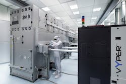
Excimer lasers cannot simply be scaled up to higher and higher powers without limit. Eventually, various practical issues, such as cooling, discharge uniformity, and beam quality, come into play. We chose a design concept in which the output from multiple lasers is combined to reach these higher power levels. Specifically, a single VYPER laser, which itself contains two separate oscillator beams, outputs 1.2kW (FIGURE 2).
A TwinVYPER laser system offers 2.4kW, which is sufficient for LTPS production on 1300mm-wide glass panels. And a recently introduced TriVYPER laser system yields 3.6kW, enabling it to process the next generation of glass panels. It's important to note that the multiple beams are not simply stitched end-to-end to produce the final line. Rather, the beams are combined first, and then shaped to their final line profile.
This beam-combining approach was taken because, in addition to simply scaling up power, it also enabled improvements in pulse-to-pulse stability, as well as allowed greater flexibility in terms of temporal pulse shaping. This is possible because the two oscillators contained in each VYPER are arranged in a master and slave configuration. Synchronization and feedback circuitry accurately controls the time delay between the pulses of these two oscillators, enabling long-term temporal stability to an accuracy of about 2ns. The arrangement allows the overall pulse length of the laser to be varied to provide pulses ranging from the standard pulse width up to essentially twice this value. This permits the manufacturer to explore the exact effects of pulse duration on the crystal structure, and to optimize the results in terms of the effects on the bulk electronic properties of the silicon.
Other high-power UV applications
The unmatched ability of excimer lasers to produce high-energy UV pulses is also benefiting other applications in displays and microelectronics manufacturing. For example, excimer lasers are used in mask-based direct patterning of microcircuits for cost-sensitive applications like medical disposables. Here, the excimer laser is used to pattern a very high volume of disposable sensor circuits in thin metal on a flex substrate in a reel-to-reel process.
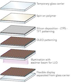
Laser Lift-Off (LLO) is another important application enabling the next generation of flexible displays. A major obstacle in fabricating flexible displays is that the thin plastic substrates employed are too delicate to be handled with traditional tooling, and will typically lose their limited rigidity at the high temperatures experienced in some production steps.
To overcome this problem, a glass substrate is used as a temporary carrier for handling purposes during fabrication (FIGURE 3). It is first coated with polymer layer and then display circuitry is created on top of this polymer layer. Finally, a high-power excimer laser beam, such as the specially designed UVblade series, is directed through the glass carrier (which is sufficiently transparent in the UV). The laser light is strongly absorbed by the polymer layer, which vaporizes and thus releases the completed flexible display from the carrier.
Conclusion
Excimer lasers continue evolve as the only practical source of very high-power UV laser light. Their unique characteristics have made them an enabling technology in a number of high-precision processing tasks, especially in display manufacturing, microelectronics, and medical device fabrication. Continuing improvement in the quality, reliability, and output characteristics of excimer lasers, necessary to meet today's demanding applications, promises to keep this powerful UV technology relevant for some time to come.
RAINER PÄTZEL and RALPH DELMDAHL([email protected]) are with Coherent, Santa Clara, CA; www.coherent.com.


