Beam profile effect for thin film solar cell scribing
In recent years, with growing concerns over global warming and foreign energy dependence, alternative energy sources such as wind and solar have garnered tremendous interest. Critical for their acceptance over fossil fuels is a low levelized cost of energy (LCOE). And, while c-Si flat panel photovoltaic (PV) modules were first to market and have been deployed worldwide, thin film PV (TFPV) solar panels have been making significant strides in furthering the widespread adoption of solar energy. Annual thin film solar cell production has increased from 17 MW in 2002 to 966 MW in 2008 with market share increasing from 3% to 14% during the same period. While 2009 was indeed a difficult year for most TFPV manufacturers, the future for this technology looks strong. New players in the market such as GE see a bright future for thin film solar technology and are investing heavily in TFPV research and development worldwide. A recent analysis by Greentech media predicts TFPV manufacturing capacity to exceed 10 GW by the end of 2012.
TFPV cells use a much smaller amount of semiconductor material—just 1-2 µm thick versus several hundreds of microns for c-Si. And, they use direct bandgap semiconductors that have stronger absorption bands, enabling TFPV cells to potentially achieve similar efficiencies. TFPV manufacturing lends itself to automated processing and better scalability. For instance, in the fabrication of TFPV panels, Q-switched diode-pumped solid-state (DPSS) lasers are used routinely to remove thin-film layers ("laser scribing") for electrical isolation of the individual segments of a monolithically integrated serial connection of solar cells.
Thin film photovoltaic solar cells
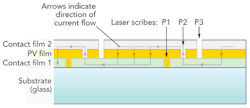
Thin film solar cells typically consist of three layers deposited on a large glass substrate: a transparent conductive oxide (TCO) layer, a middle semiconductor photovoltaic layer, and a thin metal layer (FIGURE 1). Typical semiconductor materials for thin film solar cells include cadmium sulfide/cadmium telluride (CdS/CdTe), copper indium gallium di-selenide (CIGS), amorphous silicon (a-Si) or a combination of a-Si and microcrystalline-Si (µc-Si) layers. Typical TCO materials used are indium tin oxide (ITO), tin oxide (SnO2), and zinc oxide (ZnO); typical metal layers are aluminum (Al), gold (Au), and molybdenum (Mo).
In the production of a TFPV device, three scribe processes are typically performed (commonly referred to as the P1, P2, and P3 scribes), with various film deposition processes occurring in between. The P1 scribe removes a first electrical contact film from the glass substrate; P2 scribe removes the solar absorber film from this first contact film; and P3 scribe removes both the solar absorber layer and a second electrical contact film from the first contact film. The laser scribes divide the large, meter-sized solar panels into several narrow PV cells operating electrically in series.
How beam profile affects the thin film scribe process
In TFPV processing, most scribes are performed with the laser incident from the substrate-side of the target film(s). So, any aberrations in the substrate will affect how tightly the laser can be focused, thus the laser fluence at the processing site, and ultimately the quality of the scribe. As TFPV panels scale to larger and larger substrates, glass quality and flatness will decrease as manufacturers strive to lower costs. A larger tolerance in scribe processing depths will be increasingly important for ensuring robust, high-yield scribe processes that are more forgiving of variations in glass substrate flatness, thickness, and other surface irregularities. The scribe processing depth of focus is defined as the distance along the laser beam propagation axis within which good quality scribes can be achieved with high electrical isolation. Typically, the scribing process must accommodate 1 to 3 mm depth variation. A larger process depth of focus will result in a more tolerant robust TFPV scribing process, especially as TFPV panels continue to scale.
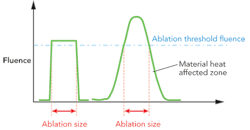
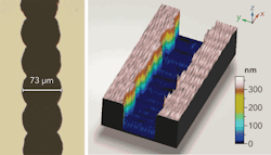
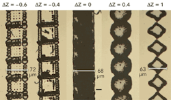
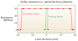
While both Gaussian and flat-top beams have been shown to produce good quality scribes, some studies have lobbied that a flat-top beam shape is desirable over the fundamental Gaussian beam shape.1 (See FIGURE 2.) For the Gaussian beam, strong ablation occurs at the center where the intensity can be significantly higher than the ablation threshold. This can result in unwanted damage to the underlying layers of the material. Furthermore, if the fluence at the edges of the Gaussian is just below the ablation threshold of the material, there can occur heating of the material at the edges, resulting in poorer quality scribes. A flat-top beam shape, however, has a uniform beam distribution, so the same amount of material will be removed across the entire defined flat-top region. Also, the sharp drop in fluence at the edge of the beam results in minimal heat-affected zones at the edges of the laser-processed region. While there are clear benefits in using a flat-top beam profile for scribing, it is unclear if there are any benefits in using a Gaussian beam profile. To explore the benefit of each scribe process, we compare P1 scribes processed using both Gaussian and flat-top beam profiles at various optical focal planes.FIGURE 3 shows a P1 scribe on 300 nm thick molybdenum (Mo) thin film on a 1 mm glass substrate achieved using a Gaussian beam from a Newport-Spectra Physics DPSS Q-switched Pulseo® 532 nm laser. Scribing of the Mo film was performed with the laser incident on the film side of the sample. Good quality ~70 µm wide scribes—complete film removal without damage to the glass substrate—were obtained by machining scribes at the focal plane.
Summary
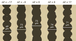
Despite a bumpy road in 2009, the future for thin film photovoltaics looks bright. Thin film solar panels are poised to gain market share in the push for alternative energy. Laser systems will play a critical part in TFPV manufacturability because they are used for scribing the thin film layers, basically "sculpting" the devices from the conducting and semiconducting layers. Choosing the correct laser with good beam quality and beam shape is critical for achieving a high-yield robust process. As we have shown here, while both Gaussian and flat-top beam can produce good quality scribes, flat-top beam processing allows <±1 mm (at most) defocus tolerance compared to ±17 mm for a Gaussian beam for ~70 µm wide scribes. Clearly, Gaussian beam machining has a significant advantage in providing a wide robust processing window—one that can accommodate 1 to 3 mm glass flatness and other variations associated with large solar panels. This is of great advantage in achieving a high yield scribing process on low cost large glass panels, ultimately leading to lower cost thin film solar cell panels.
Reference
1. O. Homburg and P. Harten, "Innovative Laser Materials Processing for Photovoltaic," Laser Technik Journal, Vol. 1, January 2009, pp. 38-40.
Rajesh Patel | Independent Consultant
Rajesh Patel, now an independent consultant in laser applications, was with MKS Spectra-Physics from 2006 through 2018, with his most recent role there being Director of Strategic Marketing and Applications Engineering.
Ashwini Tamhankar | Senior Applications Engineer, MKS Spectra-Physics
Ashwini Tamhankar was senior applications engineer at MKS Spectra-Physics (Milpitas, CA) from 2007 through 2014.
