Adam C. Tanous
Ultrafast laser technology enables true athermal ablation, setting the stage for dramatic advances in medical device manufacturing
Heat is almost always the enemy.
This is particularly true as the scale on which we build things shrinks, whether stacked integrated circuits or implantable medical devices. In the microelectronics world, the challenge is to manage—through design and materials engineering—the heat generated after manufacturing, during device operation. In the realm of medical devices, that thermal management challenge shifts to the front end.
FIGURE 1. Low and high magnification SEM images of a Nitinol stent machined by the Smart Light MD. The struts here are 92 µm across. Below, it can be seen that there are no heat affected zones.
The breathtakingly small and precise features now common in medical devices, both implantable and ex vivo, demand a new manufacturing tool—one that can machine micron resolution features without imparting heat to the rest of the part. Heat affected zones (HAZ) not only compromise device integrity, but also lower yields and increase costly post processing steps.
A solution to the problem of heat in micro-manufacturing is ultrafast laser technology, a unique and revolutionary capability to athermally ablate materials of any kind, whether metal, dielectric, or polymer. To understand why ultrafast technology offers such a sweeping opportunity, it is useful to detail how it fundamentally differs from continuous wave (CW) and long pulse (picosecond and longer) lasers.
Continuous wave lasers ablate by way of a thermodynamic process: localized heating of the target lattice followed by phase change or combustion. Femtosecond pulse lasers, on the other hand, deliver tens of microJoules of energy in 700–800 femtosecond pulses. When focused to a spot size anywhere from 30 microns down to the diffraction limit, ultrafast lasers generate extraordinarily high optical intensities. And attendant with high optical intensity is an electric field capable of initiating multi-photon ionization of the target. This photo-ionization leads to plasma formation, followed by electrostatic ejection of the target ions.
It is not enough, however, to simply ionize the target. The entire process of ionization, plasma formation, and coulombic explosion must happen on a timescale shorter than heat can diffuse beyond the volume of material being ablated.
Put simply, each pulse of an ultrafast laser removes a given chunk of material faster than the heat generated can diffuse from that localized volume to the material nearby—a sort of three-card Monte of physics. Though—like the sidewalk card game—it’s not a magic trick, simply a case of one thing moving faster than another.
And this last point underscores why the pulse duration of a given laser technology is a critical parameter; it determines whether an ablation process is athermal, thermal, or some combination of the two. Certainly, picosecond and even nanosecond pulse lasers can initiate multi-photon ionization. The dilemma is that the longer pulses allow the heat imparted by the laser to diffuse beyond the ablation volume and into the lattice surrounding the target. Even lasers with 2 or 3 picosecond pulses engage the target long enough to allow thermal equilibrium to take place. It’s this heat diffusing into the part as a whole that creates thermal damage, whether changes to microstructure, such as HAZ, melt areas, recast, or dross.
FIGURE 2. The struts of this prototype Nitinol “micro-stent” are approximately 20 µm wide. The wall of the stent is 80 µm thick. Below is a higher magnification image of the strut intersections.
For large volume material removal, these small areas of thermal damage are inconsequential. However, for very small and precise, low volume material removal—of which there are a vast number of applications—there is little or no tolerance for heat affects. This presents a wide open field of opportunity for ultrafast technology. Of course, traditionally, the problem with ultrafast lasers has been that they were big, unreliable, difficult to operate, and expensive—more suitable for scientific experiments than commercial opportunities.
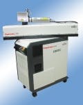
Raydiance Corporation (Petaluma, California), has taken an approach to ultrafast premised on the idea that to be useful the laser has to be practical, reliable, and capable of being readily integrated into modern production floors. On a technological level, this premise translates into a fiber architecture and thoroughly embedded computer and software control of the system.
Specifically, the company has been leveraging the athermal ablation capability of its Smart Light MD ultrafast technology to meet the very exacting machining requirements implicit in the medical devices, microfluidics, solar, and consumer electronics industries.
FIGURE 3. The struts of this prototype bioasorbable stent are approximately 80 µm wide. The wall of the stent is 150 µm.
Perhaps the most illustrative demonstration of the value of athermal ablation comes in the medical devices arena. The manufacturing of vascular stents, whether peripheral, coronary, or neurological, provides a prime example of how ultrafast technology is advancing the field.
Bare metal stents are typically made from materials such as stainless steel, Nitinol, or cobalt-chromium alloys. The stents are cylinders with diameters ranging between 2 and 3 mm and lengths from 8 mm to 32 mm. Wall thicknesses, strut dimensions, and overall design of the mesh pattern vary considerably across applications and manufacturers.
Traditional methods for machining these very fine parts—it’s not unusual for struts to be 80 µm wide—have been to use nanosecond pulse lasers. As discussed above, these lasers introduce a significant thermal component during manufacturing, which manifests itself in the form of burrs, slag, and recast. Consequently, the industry has been forced to employ costly and labor-intensive post-processing steps, such as chemical etching, to remove the imperfections. What’s more, the prevalence of HAZ in parts produced with nanosecond technology jeopardizes part integrity and, therefore, dramatically reduces the yield of the process.
The true athermal nature of ultrafast ablation enables very precise machining without the cost and complications of post-processing. Raydiance has recently demonstrated the ability to machine prototype Nitinol stents with little more post-processing than a five minute ultrasonic bath in tap water. FIGURE 1 top is an SEM image of a 700 µm diameter laser machined stent with struts approximately 92 µm wide. The stent wall is 127 µm thick. It can be seen here and in the higher magnification SEM image (below) that the edge quality of the cut is excellent, and there are no heat affected zones, slag, recast, or burrs.
The company has successfully machined still smaller Nitinol “micro-stents” with 80 µm walls and strut widths approximately 20 µm wide (see FIGURE 2 top and bottom). Again, there are no thermal effects introduced by the Smart Light ultrafast machining.
Bioabsorbable stents, which may represent the future of the stent market, are perhaps even more problematic for traditional nanosecond and picosecond laser machining. The low melting point polymers typically used in these stents, polylactic acid (Tm = 173 C - 178 C), and polyglycolic acid (Tm = 225 C - 230 C), are even less tolerant of residual heat effects than are Nitinol and stainless steel. We have done preliminary demonstrations in machining these materials. Shown in FIGURE 3 is a bioabsorbable stent machined with a Smart Light. The struts in this sample are 80 µm wide and show no signs of melt or other thermal damage.
These three examples from the medical device arena are indicative of a broader trend in micro-manufacturing. As demand for smaller and smaller parts increases—whether less invasive medical devices or consumer electronics—the athermal ablation capabilities of ultrafast lasers will play an increasingly important role in manufacturing. There are potentially huge applications for ultrafast in microfluidics and lab-on-a-chip technologies, solar cell isolation, hardened glass machining for electronic displays, and wafer dicing, to name just a few.
Just as mechanical cutting gave way to photolithography, chemical etching, and traditional and long pulse laser ablation, so too will these latter technologies cede ground to the ultrafast technology now emerging—one that is not only capable of precise, athermal ablation, but is robust and reliable enough for commercial manufacturing environments. What’s more, software control of this technology will facilitate widespread integration into automated workstations and production lines.
Adam C. Tanous ([email protected]) is director of marketing for Raydiance Inc., www.raydiance-inc.com.


