ST. FLORIAN, AUSTRIA and ARMONK, NY—Wafer bonding and lithography equipment supplier EV Group (EVG) and IBM will enter into a license agreement on laser debonding technology. EVG plans to integrate IBM’s Hybrid Laser Release process into its temporary bonding and debonding equipment solutions, which can allow high-volume manufacturers to implement optimized temporary bonding and debonding process flows.
EV Group’s laser debonding modules incorporate a solid-state laser and beam-shaping optics designed to enable optimized, force-free debonding.
The resulting advanced laser debonding solution encompasses methods and designs for ultraviolet (UV) and infrared (IR) laser debonding (designed to enable the use of glass or silicon carriers), as well as inspection of the bond interfaces. The technologies contributed by IBM help EVG implement designs that address the industry’s critical requirements for temporary bonding and debonding, including high throughput, low wafer stress for high yield, and low cost of ownership of the laser equipment, processing, and consumables. The advanced EVG solution includes techniques to help protect chips from heat and laser damage, as well as chemical clean technologies for device and carrier wafers.
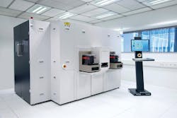
Designed for integration in the EVG 850DB automated debonding system, the company’s laser debonding modules incorporate a solid-state laser and beam-shaping optics designed to enable optimized, force-free debonding (FIGURE). Featuring both low-temperature debonding and high-temperature-processing stability, the company’s laser debonding solution is available for a variety of applications. These include fan-out wafer-level packaging (FO-WLP) and other temperature-sensitive processes such as memory stacking and integration, die-partitioning, heterogeneous integration and bio-technology/organic packages and devices applications, as well as photonics, compound semiconductors, and power devices.
For more information, please visit www.evgroup.com.
