The use of high-density packages, such as flip chips and microball grid arrays, presents new opportunities and challenges for lasers in the processing of semiconductor chips. Specifically, because the chips are no longer fully encapsulated in plastic packages, tracking and inventory controls require that marks indicating the type of chip and its lot number must be created directly on the semiconductor. This is often referred to as backside wafer marking, because the wafers are marked before dicing, and the mark must be applied to the back to avoid damaging the front-side circuitry.
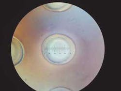
Deep, round, and clean dots provide an easily-readable debris-free mark on the wafer.
null
Laser marking has numerous advantages over alternative technologies, including high degree of permanence, cleanliness, speed, programmability and low consumable costs. However, the application of direct surface marking to semiconductors presents special challenges.
null
Advanced wafer marking
Subsurface damage is undesirable in most surface-marking applications. In the case of semiconductors, it could lead to functional damage or to a higher failure rate for the integrated circuit.
Silicon and other 3/5 wafers.
null
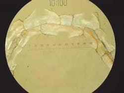
Wafer materials, like sapphire, Si, GaAs, Ge, SiC and other 3/5 materials have to be marked with a special light to prevent microcracks. For this reason an excimer laser at 193 nm is the exclusive choice in this growing application. Compared to CO2 lasers, excimer lasers don't create microcracks on the surface of the wafers.
A new type of wafer marking is used as a means of tracking wafers through process stages-polishing, coating, and so on—that would normally obliterate conventional surface marks. In the process, pioneered by Innolas GmbH (Planegg/.Munich, Germany), manufacturers use a 193 nm laser and an image mask to apply codes like OCR, BC, T7 (ECC200) and 2D on the outer area of the wafer surface. This mark endures throughout the manufacturing cycle, enabling an optical reader to view the mark at each stage. UV laser light offers strong absorption (by sapphire, Si, GaAs, Ge, SiC, GaP, InP and others) and the high resolution necessary for this application.
Powerful light
Excimer laser markers come in a variety of configurations. The laser beam can be projected through a mask and/or steered by galvanometers, then focused onto the wafer. The UV-light-source can be pulsed for dot-matrix marking. For example, the Innolas IL 2000 laser marking system is designed to mark various wafer materials such as sapphire and silicon carbide. The machine can handle flat and notched wafers from 100–200 mm without any set-up or mechanical modifications. With the four-cassette platform design, 100 wafers from one or more batches can be processed simultaneously. Combined with an ExciStar S-Industrial laser the UV-light source reaches an optimum result.
The excellent laser beam quality, stability and power provide superior marking results that meet the highest global standards. Deep, round and clean dots without microcracks provide an easily readable debris-free mark on the wafer.
Excimer lasers offer advantageous characteristics for the treatment of materials with extremely high precision and definition, producing excellent accuracy, repeatability and process control, no microcracks or chipping resulting in higher wafer yield, and the high absorption efficiency of the UV wavelength results in minimum internal stress and residual damage.
For additional information on excimer lasers contact Tui Laser at www.tuilaser.com, for laser systems, Innolas at www.innolas.de.


