Laser nanofabrication: A route toward next-generation mass production
Chen Zaichun, Chong Tow Chong, and Hong Minghui
Versatile approaches answering the call for sub-20nm industrial needs
Laser nanofabrication: A route toward next-generation mass production aser has been extensively applied in industries, such as to carry out marking, drilling, annealing, and surface modification, as a reliable energy source in cost-effective manufacturing systems.1 The development of industries now requires the reduction of feature size of devices down to submicron or even nanometer scale. As a maskless and noncontact process, laser nanofabrication has its unique advantages in a flexible setup, able to be operated in air, vacuum or liquid environment, which makes it as the most attractive processing or manufacturing tool for much more extensive applications.
A few novel techniques have been developed to make functional nanostructures. For industrial applications, the crucial issue is how to make the nanostructures over a large area in a short time for mass production. In this article, some versatile laser nanofabrication approaches for potential mass production are introduced. A vision on the further laser nanofabrication development to cater for sub-20 nm resolution is also briefly discussed.
Laser nanofabrication assisted by microsphere array
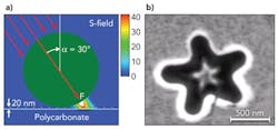
The key challenge of laser nanofabrication is how to overcome the optical diffraction limit by focusing a UV or visible laser beam in air down to sub-100 nm. Our research shows that a transparent microsphere array, formed by self-assembly or spin-coated over a large area, can split an incident laser beam into thousands to millions of tiny light beams, and also serve as the lenses to focus these tiny beams for surface nanopatterning. The localized light intensity is greatly enhanced as presented in FIGURE 1 (a) and used to process the sample in parallel mode.2 This technique employs a regular two-dimensional (2D) microsphere array to focus the incident laser beam onto the substrate. This permits the single-step surface patterning to create thousands to millions submicron holes on the substrate by only a few pulses of laser irradiation. The microspheres are removed after the laser nanoprocessing by conventional ultrasonic cleaning. Complicated nanostructure designs, such as the star array shown in FIGURE 1 (b), can be fabricated by flexibly controlling the laser beam scanning contour.3
Laser interference lithography
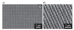
Laser interference lithography (LIL) is a powerful tool to make large-area periodic nanostructures, such as nano-dot or nano-line arrays, in a short time. With only a few minutes of UV light exposure followed by photoresist develop and chemical etching or lift-off process, plasmonic nanostructures can be created on metallic thin films. Coherent length of the laser beam is a key factor for two light beam interference over a large area (centimeter scale). Nano-line arrays are fabricated by one-time laser exposure, while further laser exposure after the rotation of the exposed sample at 90° is applied to generate nano-dot arrays. By controlling exposure time and exposure scheme, a wide variety of nanostructures can be realized, in shapes varying from rectangles to triangles to ellipses. 2D nanostructures formed on the photoresist layer can also be transferred down to the substrate by chemical etching to obtain 2.5D nanostructures. FIGURE 2 (a) presents metallic nano-dot array being embedded inside an Si substrate, and FIGURE 2 (b) shows nano-pillar array created by LIL.4, 5
Femtosecond laser two-photon polymerization nanolithography
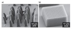
The aforementioned laser nanofabrication techniques are used to fabricate the 2D large-area nanostructures on the sample surfaces. Femtosecond (fs) laser two-photon-polymerization (2PP) nanolithography is a promising method to make arbitrary large-area 3D nanostructures. When the fs laser beam is focused into photosensitive materials, it initiates polymerization via two-photon non-linear absorption. The fs laser beam scanning profile is computer-controlled to make arbitrary designed 3D structures. The non-illuminated photosensitive materials are washed away after the laser scanning. Attributed to the light exposure threshold effect and nonlinear light absorption nature of the process, super-resolution beyond the optical diffraction limit (down to 60 nm) can be realized by flexibly controlling laser pulse energy and pulse repetition rate to make functional 3D nanostructures as shown in FIGURE 3.6, 7
Laser micro-lens array lithography
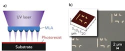
Limited by the size of the microsphere array formed on the sample surface, the nanostructures made by the laser nanofabrication assisted by microsphere array technique are typically very small, less than 1 cm2. Meanwhile, defects are introduced during the self-assembling or spin coating to form the microsphere array. Laser micro-lens array (MLA) lithography, much easier to be handled, is more applicable to mass production of nanostructures for industrial applications. The MLA splits an incident laser beam into thousands to millions of tiny laser beams as shown in FIGURE 4 (a), functioning like the microsphere array to split and focus the incident laser beam. The sample coated with photoresist is mounted on a 7-axis nano-stage and positioned at the focusing plane of the MLA. By controlling the stage movement and laser pulse on/off, arbitrary patterns are created on the photoresist layer by laser exposure. FIGURE 4 (b) shows the generic IC design array fabricated on quartz substrate.8 Laser MLA lithography has the unique advantage to fabricate large-area arbitrary nanostructures at high speed in parallel mode. This method can also be applied to make functional nanostructures on various substrate surfaces, such as split ring resonator (SRR) arrays on flexible polymer films, which can be then rolled up as a 3D meta-materials tube for ultra-sensitive sensing.
Vision of laser nanofabrication development
EUV light nanolithography and laser cooling are two highly potential means to meet industrial requirements for sub-20 nm nanofabrication. While EUV light is strongly absorbed by almost all the materials, EUV optics and photomask are very expensive and easily damaged. Successful development of multi-beam maskless EUV nanolithography via direct-writing approach is a feasible solution to overcome this technical challenge. Furthermore, laser cooling can manipulate atoms’ deposition on the substrate surfaces as these atoms pass through and are “focused” by the standing waves configured by laser beam interference to achieve feature size down to sub-10 nm. ✺
DR. Chen Zaichun is a senior teaching fellow in the Singapore University of Technology and Design, Chong Tow Chong is provost at Singapore University of Technology and Design, and Dr. Hong Minghui ([email protected]) is associate professor at the Department of Electrical and Computer Engineering at the National University of Singapore. References
1. T.C Chong, M.H. Hong, and L.P. Shi, Laser & Photon. Rev. 4, 123 (2010).
2. Z.B. Wang, M.H. Hong, B.S. Luk’yanchuk, Y. Lin, Q.F. Wang, and T.C. Chong, J. Appl. Phys. 96, 6845 (2004).
3. W. Guo, Z.B. Wang, L. Li, D.J. Whitehead, B.S. Luk’yanchuk, and Z. Liu, Appl. Phys. Lett. 90, 243101 (2007).
4. Yun J., Wang R., Choi W.K., J.T.L. Thong, C.V. Thompson, M. Zhu, Y.L. Foo, M.H. Hong, Carbon 48, 1362 (2010).
5. Choi W.K., Liew T.H., Dawood M.K., Henry I.S., Thompson C.V., Hong M.H., Nano Lett. 8, 3799 (2008).
6. T.M. Hsieh, C.W. Benjamin Ng, K. Narayanan, Andrew C.A. Wan, Jackie Y. Ying, Biomaterials 31, 7648 (2010).
7. J.K. Gansel, M. Thiel, M.S. Rill, M. Decker, K. Bade, V. Saile, G. von Freymann, S. Linden, and M. Wegener, Science 325, 1513 (2009).
8. M. Tang, Z.C. Chen, Z.Q. Huang, Y.S. Choo, and M.H. Hong, Appl. Opt. 50, 35, 6536 (2011).
More Industrial Laser Solutions Current Issue Articles
More Industrial Laser Solutions Archives Issue Articles


