Laser drilling high-density printed circuit boards
Miki Kurosawa
CO2 laser drilling has a central role in manufacturing the newest PCB materials
The ongoing, global spread of high-performance hand-held devices such as smart phones and tablet PCs has been playing a significant role in the growth of the electronics industry. Inside these devices are high-density interconnection (HDI) build-up multi-layer printed circuit boards (PCB), with electrical conduction between wirings on each layer controlled through interlayer vias. Currently CO2 laser drilling machines are extensively applied in processing of the interlayer via-holes.
The PCB material is a composite of various materials including copper foil for forming electric circuits, resin for ensuring electrical insulation, and glass fiber for enhancing mechanical strength. High-quality minute via-holes of 100 μm diameter or less are essential to the high-density interconnection of the composites. In fact, CO2 laser drilling has become central to the present HDI board manufacturing process by the development of fine quality via-hole fabrication on the composite, achieving excellent productivity and establishing economic efficiency.
In 1991, IBM introduced a photo-via technology as a practical application for manufacturing the HDI circuit board, a process where built-up layers are connected through a large number of via-holes. Although the photo-via process excels in terms of productivity, since multitudes of via-holes are collectively fabricated through the exposure process, the board material is limited to photosensitive resin. Also, in the photo-via process, the glass fibers necessary for the mechanical strength of the circuit board are not applicable, and difficulties lie in control of the chemical process. With all of those limitations, the photo-via application ended up not being widely used.
Laser drilling was then considered as an alternative technology. Initially, excimer laser and TEA CO2 lasers were proposed for the via-hole fabrication process. However, the excimer laser had challenges in terms of reliability and maintenance cost, while TEA-CO2 lasers experienced productivity problems attributed to its highest repetition frequency of only 500 Hz.
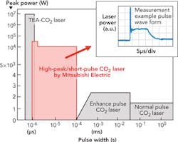
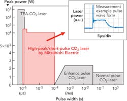
Aiming to solve the challenges of the laser drilling application, Mitsubishi Electric in 1996 independently developed a CO2 laser that could generate a pulse of over 10 kW at peak power and microsecond-order short pulse-widths, with a high repetition rate on the order of kHz. In this CO2 laser, a MOSFET-based, high-voltage and high-speed-switching inverter power supply and dielectric-discharge electrodes that produce a stable silent discharge (SD) are incorporated in the resonator's 3-axis cross-gas-flow configuration. FIGURE 1 shows the pulse range of this high-peak/short-pulse CO2 laser, capable of emitting pulse widths ranging from 1μs to some 100μs - a performance other general gas-flow type CO2 lasers have never achieved in their pulse mode operation. This unparalleled performance enables the control of thermal effects on the respective composite material of the PCB, resulting in ideal, quality via-hole processing at high throughput.
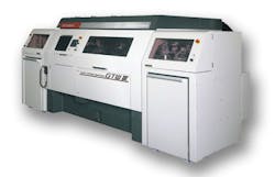
Furthermore, to tap CO2 laser capacity to the fullest, a high-speed high-precision galvo scanner system and an fΘ lens are combined with the CO2 laser drilling machine shown in FIGURE 2. In this laser drilling system, the laser beam is spatially divided by a beam splitter into two equal beams which are delivered to two processing heads equipped with the galvo scanner and the fΘ lens, enhancing productivity through the simultaneous processing of two PCB panels.
FIGURE 3 shows examples of copper direct drilling that is commonly performed in the HDI board manufacturing process. This drilling is a blind via process where a laser penetrates a surface copper foil, drills a resin layer, and stops on the surface of a cooper inner layer. In copper direct drilling, a quick shot of the high-energy laser pulse to a processing spot is necessary since copper is a highly thermal-conductive material. The CO2 laser, with its characteristically high-peak-power laser pulse, is able to process on the surface copper foil with good performance, and fine-quality blind via holes with smooth wall surfaces do not lower the integrity of a plating process performed after the laser drilling. At present, 2-head type CO2 laser drilling machines can perform the copper direct process at a throughput of 1,500 holes per second. More than 3,000 units of this type machines are now in operation mainly in Taiwan, and also in China, Korea, and Japan for the copper direct processing of the HDI boards for smart phones.
In addition to the HDI board manufacturing application, the CO2 laser blind via drilling process is applied to manufacturing a semiconductor package where the silicon IC chips are mounted. The semiconductor package constitutes two types of layers: a core layer to ensure the board rigidity, and a build-up layer for forming superfine circuits of electrical interface with the silicon IC chip. Due to the high integration of the silicon IC chip, the semiconductor package must incorporate higher-density interconnection circuits. In this domain, the technology requires the fabrication of a blind micro via of ≤50 μm diameter on the build-up layer and a small through-hole of ≤100 μm diameter on the core layer. FIGURE 4 shows CO2 laser drilling examples of the blind micro via and the small through-hole.
As for the blind micro via, a process of 40 μm-diameter-class blind via holes performed by UV lasers, has been demonstrated by the CO2 laser drilling machine through the installation of the high-performance fΘ lens whose optical aberration is reduced to the minimum. Furthermore, this latest laser drilling machine is able to process four holes at the same time with split four laser beams, and it achieves high throughput of 4,500 holes per second. This micro via hole processing by the CO2 laser is more economically efficient than the UV laser, proving its contribution to reducing the manufacturing cost of the high-end semiconductor packages.
Concerning the through-hole process, a laser-drilling method different from that of the blind via process has been adopted on a board with a copper layer on both the top and bottom sides. This method includes laser drilling to the middle of the board from one side first, then flipping the board and drilling from the other side in the same position to create one through-hole. Typical laser drilling galvo position accuracy is less than +/-10 μm, enabling drilling of <100 μm-diameter through-holes without displacement between the double-side drillings. Since the laser through-hole drilling can solve problems of conventional mechanical drilling - namely its drill bit cost, productivity, and hole position accuracy - the laser through-hole drilling technique is rapidly becoming prevalent.
CO2 laser drilling is applied not only in electrical circuit board fabrication, but it is also widely in the manufacture of a multi-layer ceramic capacitor (MLCC) used in large volumes for hand-held devices. In case of the MLCC, a ceramic sheet before sintering, called a "green sheet", is a target material for the laser process. The high-peak/short-pulse CO2 laser is appropriate for high-speed fabrication of high-quality, extremely minute holes on the green sheet. Some hundreds of the Mitsubishi Electric CO2 laser drilling machines are operating in the MLCC manufacturing sector as an indispensable production tool.
Along with the overall intensifying cost-driven trend in semiconductor package manufacturing, CO2 laser drilling is attracting attention from the semiconductor packaging industry. Although the CO2 laser is not necessarily the cutting-edge with new lasers being introduced one after another, it is certainly an excellent, reliable and economical laser in terms of industrial applications. No laser technology that is technically outstanding but less reliable and less economical can become central to the industrial process. From this point of view, CO2 laser drilling is presumed to further its development as a useful tool in the PCB manufacturing industry.
Miki Kurosawa ([email protected]) is the manager of the laser micro-processing systems design section of the laser systems department of Mitsubishi Electric Corp., Nagoya Works, Nagoya, Japan.


