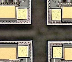
The tight, narrow, clean cuts achievable with UV laser scribing provide better die count per wafer and higher yields due to fewer damaged die
Precision scribing of wafers with ultraviolet (UV) lasers has emerged as an alternative method of scribing for separation, particularly for brittle compound semiconductor wafer materials such as thin silicon wafers. UV diode-pumped solid-state (DPSS) lasers rapidly process wafers with kerfs of less than 3 microns in thin or thick wafers without edge chipping in all the III-V materials, including IV materials such as Silicon (Si) and Germanium (Ge), and straight, accurate, cleaner cuts particularly for Gallium Arsenide (GaAs) wafers. GaAs wafers are expensive, so wafer real estate is valuable. The tighter, narrower, cleaner cuts achievable with UV laser scribing provide better die count per wafer and higher yields due to fewer damaged die. The laser scribing process operates within 20-micron streets or narrower.
High-frequency electronics that use GaAs chips require accurate mechanical placement of chips to minimize air bridges and impedance mismatches. Straight, accurate chips allow greater precision in die placement and better overall packaging and electrical performance of the die.
Increasing challenges
Die are constantly being designed to be smaller because the market is driving the cost per die ever downward. The decrease in die size is creating new problems with the scribe-and-break process. Dicing lane widths have been reduced from 100 to 30 microns and die sizes are shrinking. Thirty microns is past an acceptable limit for the traditional saw process. With laser scribing, the street can be further reduced to 15-20 microns. In addition the area referred to as the “zipper” (a place to stop any surface cracking) can be removed. The area gained from street reduction, removal of the “zipper,” and following design rules is ~24 microns per side of each die. This accounts for a large area on the entire wafer.
With GaAs wafers, the breaking process is described as being either non-contact (exposed air bridges) or contact break. Each break method has an aspect ratio, defined as length/width of die over thickness of die, listed by the tool manufacturer. For one particular saw dicing scribe-and-break system the aspect ratio is listed as 7:1 for non-contact breaking, and 3:1 for contact breaking.
The decrease in die size has reduced the aspect ratio of some products to 2:1, effectively pushing the limits of the listed capabilities of the mechanical scribe-and-break system. These chips occasionally take a high yield hit due to non-separation. Saw dicing is slow and causes chipping at the edges of the die, sometimes ruining the die. The narrow (30 microns wide) street requires an extremely narrow saw blade that wears easily.
Better yields with UV lasers
The use of short-wavelength (157-248 nm) excimer and UV DPSS lasers has increased die yields and has also proven superior to traditional diamond scribing. UV laser processing allows a much narrower scribe kerf (material lost in the scribe) width than other technologies. This, coupled with front-side processing, increases the number of usable die that can be produced per wafer.
New short pulsewidth, short wavelength UV-DPSS lasers offer a wide range of flexibility in terms of modifying pulse shape, repetition rate, color, beam quality, and much more. Harmonic generation allows the use of shorter wavelengths for a wide range of materials processing capabilities. DPSS lasers offer excellent beam quality and the highest repetition rate while providing the smallest beam size for micro features. Typically the DPSS lasers used at JPSA are vanadate (Nd:YVO4) based and produce an infrared (IR) beam at approximately 1 µm. Efficient frequency conversion allows us to use these lasers at 355 nm and 266 nm with several watts of available power.
The development of these lasers makes them particularly suitable for dicing applications. At JPSA these lasers are used to dice blue-LED (light emitting diode) and sapphire wafers at speeds of 75 mm/sec, leading to a throughput of more than 9 wafers per hour (for standard 2-inch diameter wafer with die size of 350 µm x 350 µm) while creating a very narrow kerf (<3 µm). With its high throughput and minimal impact on LED performance, the process is tolerant of wafer warp and bow, and delivers much faster scribing speed than traditional mechanical methods. For III-V semiconductors, such as GaAs and Indium Phosphate (InP), a cut depth of 40 µm is typically achieved at speeds higher than 150 mm/sec.
Excimer lasers offer maximum power and the shortest wavelength (351, 308, 248, 193, and 157 nm) of all narrow-band UV sources. The cost of photons is less compared to a DPSS laser, however the excimer system’s greater complexity, maintenance issues, and other considerations make it a less desirable choice for wafer dicing. The excimer’s strengths are in micromachining, large-area patterning and step-and-repeat processing of massively parallel areas. The UV-DPSS laser is better suited to scribing. With an excimer laser (193nm), JPSA processes three wafers per hour at a cost of $8 per wafer, with 97 percent uptime; this is very good performance for an excimer laser system. An optimized UV-DPSS (266nm) produces 7 to 10 wafers per hour at less than $1.50 per wafer with >99.9 percent uptime. These processes have both been tested over multiple installations with 24/7 operation over 1.5 years, and even longer for excimers alone.
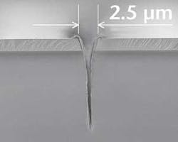
SEM of deep V-groove created by UV laser scribing. Kerf width is only 2.5 microns wide at the top.
The method of materials removal is known as laser photoablation, a process that occurs when small volumes of materials absorb high peak power laser energy. When matter is exposed to focused UV laser light pulses, the energy of the pulse is absorbed in a thin layer of materials, typically <0.1µm thick, due to the short wavelength of deep UV light. The high peak power of a UV laser light pulse, when absorbed into this tiny volume, results in strong electronic bond breaking in the material. The molecular fragments that result expand in a plasma plume that carries any thermal energy away from the work piece with little resulting damage to the surrounding material. Each laser pulse etches a fine sub-micron layer of material; the ejecting material carries the heat away with it. It is much finer and less in volume than, for example, the rough by-products of mechanical scribing, and is easily removed.
One key misconception is that the “break” after laser scribing requires more deformation of the wafer than with diamond scribing, leading to a break that is less “clean.” Actually, diamond scribing produces mechanical stress throughout the entire process. Non-mechanical and non-thermal laser scribing produces no stress on the material at all. The sharp V-groove of the UV laser-generated kerf results in a high stress concentration at the tip, which breaks very easily. Users report improved electrical performance of devices thus separated.
Laser processing advantages
With the scribe-and-break process, Process Control Monitoring (PCM) structures must be designed with through-dicing lanes. The diamond scribe does not scribe continuously through the structure. Thus, the structure must be designed with dicing lanes. This creates issues for the testing of these structures. However, with laser scribing, PCM design is no longer an issue. The structures can be designed in a way that benefits the tests being completed, not to the requirements of the separation method. Laser scribing is not interrupted when there is no dicing lane.
When using traditional methods of separation, the dicing lanes must be free of thin films or metal. With the saw process, thin films/metal in the dicing lanes increases wear on the blade, thus reducing the life of the blade or possibly causing the blade to “blow” during the cutting process. With scribe-and-break, thin films or metal in the dicing lanes causes the diamond tool to skip or bounce, creating areas that are not scribed. These areas therefore do not break, which can cause the rest of the wafer to break off the scribe lines. Thin films or metal in the dicing lanes do not limit laser scribing. The ability to dice through thin films may increase throughput for the photo processes as well. Currently, all wafers must be patterned to the edge of the wafer, including partial fields, so that the street can be etched clean, creating a clean dicing lane to the edge of the wafer. When the wafers are not patterned to the edge, the yield drops significantly.
The diagram illustrates the process of photoablation by pulsed UV laser.
Traditional methods of die separation require more time. For example, a wafer with a die size of 0.300 mm x 0.360 mm x 4 mils thick has ~55,000 die. A wafer with this die count takes ~4 hours to scribe via saw (saw speed = 6.5 mm/sec), ~2 hours with scribe-and-break (scribe speed = 12.8 mm/sec), or ~3 minutes with laser scribing (laser scribe speed = 150mm/sec). Thus, the throughput of one laser scribing system can replace and exceed the capacity of all current die separation tools combined.
Laser scribing provides the added benefit of more options when choosing shipping methods. The scribe-and-break process requires that wafers are scribed on a film frame and then transferred to a grip ring for shipping. Wafers that have been scribed must be stretched to prevent the die from rubbing together when the tape flexes. Many customers require the wafers to be on a film frame; or, customers must make modifications so that the wafers can be received on a grip ring. Laser scribing provides the option of shipping wafers on a film frame. The die are separated through the active levels by laser scribing. The die will only rub together in non-active material.
Current die separation methods lose some yield due to chip-outs. Chip-outs are eliminated with laser scribing. This fact alone has a significant positive impact on product yield.
Laser scribing increases wafer throughput on final automated wafer inspection. Currently, wafers must be stretched to prevent potential chip-outs caused by the die rubbing together. The die do not stretch uniformly, so this contributes to a lengthening of inspection time, because each die must be individually aligned for automatic inspection to be performed correctly. Occasionally, yield is impacted because the die will not align. Laser scribing allows wafers to be inspected on a film frame, which greatly reduces inspection time and allows all products to go through the auto inspection process.
Conclusion
-Advantages of UV scribing over mechanical scribing are multiple. These include lower consumables costs, less maintenance, higher throughputs, and more efficient use of floor space. The laser process is more readily automated, thus lowering labor costs. UV laser technology has greater yet-unrealized potential; thus, processes will continue to improve. We predict that there will be further improvement in terms of die count per wafer and faster economic payback with UV lasers.
Dr. Jongkook Park is with J P Sercel Associates Inc. (Hollis, NH; www.jpsalaser.com) and Jennifer Welborn is with MA/COM (Lowell, MA).


