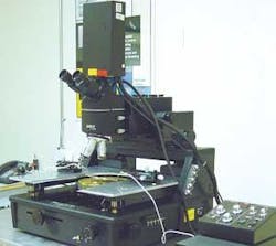
The use of a low-power, Nd:YAG laser for circuit modification has become a common tool in the semiconductor industry. Mounted on an analytical contact probing station (see Figure 1), the laser is used for failure analysis of new and returned devices to isolate faulty components by cutting the traces (metal lines) that connect them to the rest of the circuit, to remove passivation over the circuit to provide access to circuit traces and connections, and to dig through multiple layers of interlayer dielectrics and even metal allowing electrical contact to be made to buried circuit paths.
The first laser that could be mounted on a probe station for semiconductor failure analysis was introduced by Alessi Corp. in the early 1990s. Using a single wavelength (1064 nm) pulsed laser, this product had clear advantages in precision and cleanliness of the circuit cut. It was much better than the previously used technology, an ultrasonic cutter probe, which was difficult to use on the emerging sub-micron circuit geometries. The laser could be mounted on and focused through the microscope of an analytical probing station, which meant that the circuit could be modified while probing was going on. This made for a big improvement in failure analysis efficiency. The product was chosen as a breakthrough product of the year.
The Micromanipulator Co. Inc. (Carson City, NV; www.micromanipulator.com) developed an improved version of the laser cutter, adding a Q-switch, beam attenuation, and an improved mounting system on the probe station microscope for accurate targeting. The Q-switch increased power uniformity and provided a short burst (10 ns) of power to the device under test. This minimized melting of the sample and provided a cleaner cut. By attenuating the beam instead of changing power to the flashlamp, power control became more linear and repeatable. The improved targeting feature was understandably one that was strongly welcomed by the industry. In addition, the laser frequency was doubled, providing a green (532nm) wavelength. This allowed for removal of more materials, including passivation and interlayer dielectrics.
New Wave Research Inc. (Fremont, CA; www.new-wave.com) then took the laser cutter the next step with a system that included an adjustable rectangular aperture to allow rectangular cuts and a visible targeting illuminator beam that shared the laser optical path. These improvements allowed cuts to match the layouts of the semiconductor circuits and also provided the ability to see the size and shape of the cut before actually firing the laser. New Wave also tripled the laser frequency to provide a 355nm (UV) wavelength. Their new offering even allowed the user to select the wavelength from the root beam wavelength (1064 nm), or the frequency-doubled (532 nm) or tripled (355 nm) wavelengths with the rotation of a switch.
Today’s laser cutter contains all the above features. It is a relatively low-powered laser, because the materials to be removed range only from a few hundred Angstroms to a few microns in thickness. The typical laser used for semiconductor failure analysis today carries the specifications shown in Table 1.
Uses
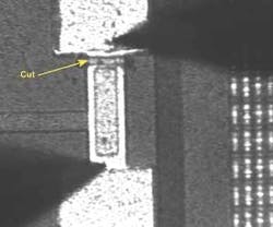
The primary use of the laser is to cut metal lines to isolate failed components. Figure 2 shows an example of a metal line that has been cut using a laser. This technique is used to “surgically” remove a suspect component, for example a transistor, from a circuit. Often, a component will be damaged and will “pull” too much current. This will cause the voltages throughout the circuit to be low in magnitude. The circuit lines that connect to the component that bring power to it and carry its output on in the circuit are cut while the device is being probed on an analytical probing station. As soon as the damaged component is isolated by the laser cuts, the circuit voltages can return to normal, confirming that the removed component was the culprit.
However, probing the circuit itself can present a problem. The need is to place the small electrical contacts (probes) on the circuit traces so that the voltage and currents of the circuit can be monitored. The problem is that the traces to be probed may be close to the top surface of the I.C., or they may be buried several layers deep under criss-crossing layers of circuit traces. These crossing conductors are separated by insulating “interlayer dielectric” layers.
The laser cutter can be used to solve this problem. By choosing the correct wavelength, varying the spot size, and applying the right power setting, the top covering (passivation) over the circuit can be removed, then interlayer dielectrics can be removed providing access to the traces for probing.
Table 2 shows some common materials that are removed by the different wavelengths.
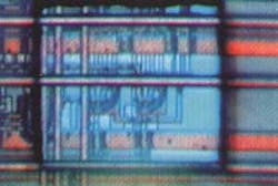
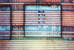
The Failure Analyst starts with the UV wavelength and a large spot size and removes the polyimide passivation to expose the traces that are at the top layer of the circuit to be probed (see Figure 3). If the trace to be probed is not on the top layer, then the spot size is reduced so that other circuit traces are not damaged, and a hole is cut through the interlayer dielectric (see Figure 4). This exposes the underlying metal that needs to be probed.
SEM images have shown “drilling” through the successive layers and materials with decreasing spot sizes. This suggests another advantage of laser cutting through multiple layers. Not only does the hole to the underlying metal provide access to the trace, but it actually can be used to “guide” the probe to the trace and keep it in place. The sharp probe point pokes into the hole to touch the trace and stays in place (see Figure 5).
The fact that the material removed by a laser cutter is limited is another advantage. Interlayer dielectrics and crossing traces create capacitive paths in the circuit. The removal of too much material can alter circuit performance. In some cases this can make a problem, such as a signal timing or “race” condition, actually disappear because the circuit properties are altered.
Finally, the laser can even be used as a “marker.” The location of the damaged part or defect can usually be found by probing and testing the circuit. At least its location can be narrowed down to a small area. However, the actual cause of the defect may require the use of a SEM or other tool to identify. In this case, the laser cutter can be used to mark a “path” to the defect location. A series of laser cuts can be made leading to the area of the defect. Then, the SEM operator can follow the path to the suspected defect and search the correct area quickly.
Once a luxury, the laser cutter has become a ubiquitous tool in the failure analysis of today’s semiconductor circuits. Its precision, repeatability, and flexibility provide the necessary capability to match the high density and small geometry circuits of today.
Mike Jackson is the director of sales and marketing for the Micromanipulator Co. (Carson City, NV). He can be contacted at [email protected].


