Pulsed nanosecond fiber lasers can weld, too!
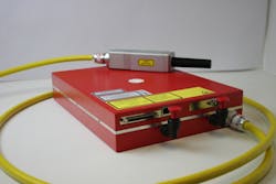
The versatility of pulsed nanosecond (ns) infrared fiber lasers is well known, as they are the laser of choice for the majority of industrial marking and engraving applications. Having typically less than a few millijoules in pulse energy and up to 100W of average power, they pack an impressive punch, with high pulse repetition rates and continuous-wave (CW) and modulated quasi-CW (QCW) modes. More recently, they have begun to be used for a variety of micromachining and surface texturing applications and even for remote microcutting applications. The vast majority of these applications involve material removal. Based on this premise, considering this beam source for material joining is counterintuitive. To consider that the same source can join material as well as remove, ablate, engrave, cut, and mark is truly impressive (FIGURE 1).
To a laser user, the benefits are significant, offering access to a laser source that can multi-task as well as be packaged in a compact, often air-cooled form factor, making integration seamless. Conventional wisdom suggests that long millisecond-type pulses with large pulse energies are needed to create welds and joints—well, evidently not! The capability of this genre of laser for materials joining is less well known, but their ability to join thin section materials is remarkable.
Globally, industries such as consumer electronics, energy storage, and medical devices increasingly package more features into smaller-volume, high-density packaging. With that, there is also an increasing need to create effective manufacturing technologies to make these products a reality; in this case, with laser joining technologies. So there is a production technology that offers the required high reproducibility, accuracy, and productivity with the all-important low cost (capital and maintenance)-industrial (nanosecond infrared fiber) lasers that meet the demands of the market.
A variety of laser types have all found their places, from pulsed YAG, disk, fiber (CW and QCW), and even diode, depending on the application. Until now, the use of nanosecond pulsed lasers has been limited to a few pioneering applications—but things are changing, with recent applications demonstrated using nanosecond fiber lasers for material joining.
SPI has been a pioneer in the introduction of master oscillator power amplifier (MOPA) nanosecond fiber lasers, which have been viewed as extremely versatile tools because of their ability to control and tailor the pulse characteristics to the requirements of applications. This is achieved through the ability to change the pulse duration and also the pulse frequency, with some sources able to operate from 3 to 500ns. Their ability to switch between pulsed and CW operation has also been an important differentiator, as has the availability of these laser sources in a range of different beam qualities, providing tools that can be adapted to the job in hand. Within the range of the average and peak powers, this laser can be modulated in the millisecond regime for applications that demand a millisecond pulse of low average power.
Plastic welding
Take plastic welding, for instance: some applications where precision is required, such as microfluidic devices, benefit from the use of a fiber laser over other sources. The energy profile in the spot can sometimes make the difference. For example, in a complex medical device, where the requirement was to weld a transparent polymer to a black one, a 40W M2=3 laser beam was used in CW mode (FIGURE 2). "It gave me the control of the beam in terms of spot size, energy distribution, and depth of field that I required," commented Joe Lovotti, director of laser technologies at Okay Industries (New Britain, CT).Wire welding
With regard to metallic welding, the medical devices industry is constantly coming up with micro-joining applications that challenge even the best of application engineers. The joining of fine wires is just such an example where CW fiber lasers have been extensively used. However, as the wires became smaller, the challenges associated with thermal input have increased. The use of a 20W laser with an M2 <1.6, giving the fine focus for the welding of a 50μm coiled wire, was found to provide an excellent result. The challenge was to suppress the peak power in the pulses by operating the laser at higher repetition rates, creating more of a QCW with <0.1mJ pulses at frequencies >250kHz—a short burst is all that's needed.
Some applications require the joining of a covering sheath or braid to a wire (FIGURE 3). Here, it was found that having a broader energy distribution in the pulse created a better wetting regime between the two parts. In this example, a 40W M2=3 laser was used where the larger spot and the slightly higher pulse energy of >1.25mJ helped bridge the gap.On the other hand, the use of a 20W single-mode laser with M2 <1.3 can demonstrate the extraordinary precision that can be achieved. An example is the welding of fine dissimilar wires of 12μm diameter, which have been successfully welded to form a thermocouple. In such applications, the jigging and vision system are as important as the laser in achieving the desired result.
Soldering applications
For soldering, CW or direct-diode lasers are typically used, but in applications where the heat input is critical, pulsed lasers can be considered. By using long pulses at high repetition rates, improved energy utilization efficiency can be achieved, reducing the risk of thermal damage. By using a scanner-based beam delivery system, the laser energy can be deposited over a larger targeted area such that the gold/tin solder paste in the example shown is only melted on the contact (FIGURE 4).Metallic welding and joining
Using nanosecond pulsed lasers for welding metals needs careful adjustment of the pulse conditions and the process setting to actually achieve good joints. After all, the prime application of these types of pulses is to remove material not to melt and allow it to resolidify. The pulses are optimized to give a maximum peak power and pulse energy, but these characteristics can be modified by using them at higher frequencies. This has the effect of reducing the peak power and moving the output closer to a QCW gated pulse while maintaining the average power.
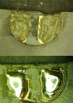
At these higher frequencies, the pulses move from an ablative to a more melting interaction with materials. The effect can be dramatic, as can be seen in the example below when using a 70W laser to make some 6mm diameter "bead on plate" rings in thin stainless steel sheet. Using a 250ns, 1mJ pulse at 70kHz, the result is extremely rough and highly oxidized. Keeping all the parameters the same but just by raising the pulse frequency, a significant improvement can be seen. By doubling the frequency to 140kHz and halving the pulse energy to 0.5mJ sees a reduction in roughness and oxide, but by increasing the frequency to 500kHz and reducing pulse energy to <0.15mJ, a bright, shiny weld can be achieved, even without a shielding gas. Using this technique, lap welds in 250μm are possible (FIGURE 5).Weld shape can be further improved by using wobbling techniques to widen the weld and improve weld penetration at the expense of welding speed.
Tests completed on stainless-steel-to-stainless-steel welds show shear strength for two 1mm welds in a full 0.5mm lap weld to be > 224 lbs. In one case with a 180-degree peel test on a linear weld 5mm long and 1mm wide, the part yielded at 241 lbs (FIGURE 6).In fact, this technique can be used on a wide variety of other metals such as steel, aluminum, and even copper. In the use of this technique for joining highly reflective materials, the pulses need to be tuned to give sufficient pulse energy to couple into the material. Spot welds of any diameter can be achieved by using a spiraling technique; for example, three 1mm spots can be created to join 150μm-thick copper foils in well under a second with a 70W EP-Z laser. Then, the challenge was to see if dissimilar metals could be joined.
Dissimilar metal welding
A typical requirement is the joining of thin copper foil to aluminum most commonly found in electronics and battery applications. Having been sent this challenge, SPI's applications team went to work. They soon reported success and when asked how strong the welds were, they responded with a picture of the weld supporting a 12lb static load (FIGURE 7).In fact, recent validated testing carried out on a tensile test machine show that the copper to aluminum joint fails at 26lbs in shear with a 90 degree peel test that yielded at 6lbs. The weld(s) remained intact.
It has been demonstrated that more challenging dissimilar materials have been welded for real commercial applications (FIGURE 8). "Using just a 20W single-moded nanosecond pulsed laser gives us a lot of control over heat input and weld geometry in a competitive and compact package for particularly challenging micro-welding applications, such as this stainless steel 0.1mm foil to 0.25mm titanium foil," says Dr. Geoff Shannon of Amada Miyachi America (Monrovia, CA).The introduction of multi-application tools for streamlining production lines is gaining momentum in, for example, medical device manufacturing. "These fiber lasers represent a revolutionary tool that can trim, etch, polish with nanosecond pulses, and weld with multi-millisecond pulses, all done with the same laser during the same production activity," comments Mark Brodsky of the Laser Mark's Company (San Jose, CA).
Conclusion
This article has shown that a number of applications, from plastic bonding and soldering to thin sheet metallic welding and wire joining, where the use of nanosecond pulsed fiber lasers are proving to be an excellent alternative to conventional millisecond pulsed YAG and modulated CW laser sources. The adoption of these laser sources in multi-process manufacturing is further testament of their versatility.
About the Author
Jack Gabzdyl
Industry Manager – Electronics, TRUMPF Laser UK Ltd
Dr. Jack Gabzdyl is Industry Manager – Electronics at TRUMPF Laser UK Ltd (Southampton, England) and has more than 30 years of laser materials processing experience. He obtained his PhD in laser processing from Imperial College London in 1989. He has since had a number of technical and marketing positions at BOC Gases, Advanced Laser Solutions, and TWI before joining TRUMPF (formerly SPI Lasers) in 2007.
Daniel Capostagno
Applications Manager - Americas, SPI Lasers
Daniel Capostagno is Applications Manager – Americas at SPI Lasers, Santa Clara, CA.


