Laser ablation delivers higher throughput and better yields
RALPH DELMDAHL and MATTHEW GINGERELLA
The relentless consumer demand for microelectronics products that are more compact, energy-efficient, and deliver greater functionality translates into a need for circuit packaging techniques employing ever-smaller feature sizes. Traditional methods (e.g., photolithography) used for a variety of microstructuring tasks in advanced packaging are becoming less effective and more costly as circuit dimensions shrink, so excimer laser ablation offers an attractive alternative in many cases. This article looks at the use of excimer laser ablation for drilling glass interposers, and reviews how excimers have been successfully employed in a turnkey platform from SÜSS MicroTec (Corona, CA) for other advanced packaging applications.
2.5D and 3D packaging
So-called "3D packaging" is an important emerging technology for achieving higher density of packaged microelectronics. In 3D packaging, multiple individual integrated circuits (ICs) are stacked like a sandwich. An interstitial substrate serves as an interconnector and redistribution circuit between the dies. This substrate, called an interposer, might be constructed of silicon or glass. Currently, actual microelectronics production utilizes 2.5D packaging. This is an intermediate step where just a single set of circuit dies is stacked on the interposer.
A critical process is the creation of small through-holes (vias), which are used to make electrical connections between the circuit components. Target via diameters are currently in the 25μm size range. These vias can be produced using several techniques, including photolithography, etching, sandblasting, ultrasound drilling, or laser ablation.
Laser ablation offers advantages over other methods because it is non-contact, scalable, and enables the production of small, high-precision features on a wide variety of materials. Furthermore, laser microstructuring often delivers higher process throughput and better yields with superior process consistency. Plus, it is an inherently "greener" process, avoiding the use of potentially hazardous lithography chemicals.
Because of these benefits, CO2 lasers have been used extensively for drilling vias in microelectronics packaging applications for some time. However, the long infrared wavelength of CO2 lasers limits their minimum focused spot size (due to diffraction). The result is a practical lower limit of about 70μm for the diameter of CO2 laser-drilled vias. Reaching smaller diameters therefore requires a shorter wavelength (e.g., ultraviolet) laser.
To investigate the potential for using excimer lasers for this application, the Coherent applications laboratory test-drilled a large number of tightly spaced holes into glass wafers. Specifically, these were 25μm diameter holes, with a pitch (hole-to-hole spacing) of 50μm, produced in glass substrates ranging in thickness from 100 to 300μm. They used a 193nm laser wavelength with a 600mJ pulse energy in a mask-based process that produced a fluence of 7J/cm2 at the work surface. The 193nm wavelength was chosen because glass exhibits strong absorption at this wavelength.
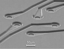
Clean, round, symmetric vias were successfully produced in all the thicknesses tested using a total of 700 pulses or less. Hole taper was seen in the higher thicknesses, but sequential drilling from both sides of the glass reduced this effect substantially. This is relatively easy since the transparent glass makes it easy to register fiducial marks on one side of the glass when it is flipped over for drilling from the second side. Overall, this testing showed that vias down to 5μm diameter could be successfully produced (FIGURE 1).
Another attractive feature of excimer interposer drilling is that it is implemented using mask projection. In this approach, laser fluence, pulse frequency, and total pulse count dictates the maximum field size that can be used, but not the total number of holes that can be produced within this field. Thus, as pitch size decreases (and the number of holes produced in a given area increases), parallel, mask-based drilling becomes increasingly efficient. In fact, the parallel drilling rate increases with the square of the pitch size. This tends to "future-proof" the technique as via diameter and pitch decrease over time.
Structuring polymers for RDLs
Virtually all types of advanced packages, such as flip chip, wafer-level chip scale packages, fan out wafer-level packaging, embedded IC, and 2.5D/3D, require redistribution layers (RDL). These are defined by the addition of metal and dielectric layers onto the surface of the wafer, which re-routes the input/output layout to match the pitch on the intended substrate.
Currently, much of the industry fabricates RDL using "photodefinable" dielectrics. These are photosensitive materials that are lithographically exposed with the desired circuit pattern and then wet-developed to remove either the exposed or unexposed areas.
Unfortunately, photodefinable polymers are costly and the photolithography process involves multiple expensive wet-chemistry steps. In addition, these materials don't always have ideal electrical and mechanical performance properties due to the inherent photosensitive additives. For example, the coefficient of thermal expansion (CTE) may not match that of the material to which they are to be bonded, resulting in mechanical stress. Therefore, the use of photodefinable dielectrics may result in warpage and stress problems, which can cause failures at the chip/package interface. All these issues become more critical as RDL features shrink and densities increase.
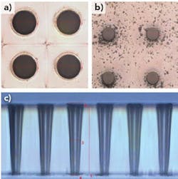
A solution to the shortcomings and high cost of photodefinable dielectrics, and their related processing, is to use a suitable non-photo dielectric material and incorporate direct excimer laser patterning. The adoption of non-photo dielectrics is an attractive solution because many formulas cost about half as much as photodefinable versions. In addition, many non-photo dielectrics produce less stress, lower CTE, and have vastly improved mechanical and electrical properties. Excimer laser ablation is the cost-effective patterning method for non-photo dielectrics and advanced composites, such as silica-filled epoxy mold compounds. It involves fewer steps than photodefinable dielectric patterning and eliminates wet chemicals for an overall "greener" process (FIGURE 2).
The SÜSS MicroTec ELP300 is a commercially available tool for performing excimer laser ablation in advanced packaging production. The system utilizes a typical mask-projection, stepper-type configuration. Specifically, the laser is projected through a mask containing the desired pattern to be produced, and the substrate (which is larger than the projected pattern) is ablated, moved, and then ablated again, until all the desired areas have been patterned.
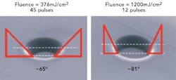
This system is available with either 308 or 248nm excimer lasers, allowing it to be matched to the absorption characteristics of the particular materials in use. The high pulse energy (over 1J) and repetition rate (300Hz) provide rapid throughput of feature sizes down to 3μm. In addition, excimer laser ablation provides excellent control of feature depth and "wall angle." The latter is important because subsequent metal sputtering or vapor deposition processes can be degraded by "shadowing" on the sides of steep angled features (FIGURE 3).
Seed metal removal
Another unique advantage of excimer laser ablation is that it does not affect copper or aluminum layers above 1μm thick. But conductive layers thinner than about 500nm are easily ablated. This inherent behavior can be exploited in a very useful way.
Traditionally, RDL conductive structures are built up in a multi-step process. To start, the entire device surface is coated with a thin layer (<500nm) of metal by sputtering or vapor deposition. This "seed" conductive layer is then covered with a dry film, which is patterned lithographically, followed by electroless plating to build up the conductive structures to their final thickness (usually >1μm). The photoresist is stripped and finally, the seed layer is removed by either plasma or wet chemical etch, leaving just the thicker metal structures.
Both of these etch techniques have several drawbacks, including the etching and undercutting of features that can make them mechanically unstable and lead to device failure. Wet-etch methods can even cause metal to leach into the dielectric material, leading to electrical shorts. Plus, etch processes have low throughput, use hazardous chemicals, and aren't environmentally friendly.
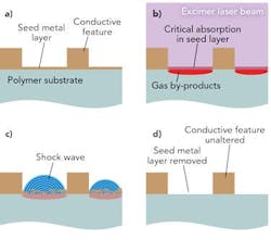
In contrast, excimer laser seed layer removal is a dry, one-step process for wafers with organic passivation layers below the seed metal. After plating and resist stripping, the entire wafer surface is exposed to a single excimer laser pulse. The thick metal conductive structures readily disperse the laser energy in all directions within their lattice structures and do not ablate. However, the thin seed layer cannot disperse the energy fast enough and it surpasses the metal's ablation threshold. The absorbed energy creates molecular vibration and heat within the seed layer that reaches the polymer interface, breaks bonds, and produces gas by-products. The gas pressure at the enclosed interface has nowhere to go until the laser-pulse shock wave reaches it and is redirected upward to blow off the overlying thin metal layer. This "spallation" occurs with minimal damage to surrounding and underlying materials (FIGURE 4).
Excimer laser seed metal removal prevents undercutting and etching of plated metal structures, eliminates wet etch chemicals and related costs, is a simpler dry process, and even allows for recovery of the ablated metal. Plus, the excimer-based process is fast. For example, when using a high power excimer laser (e.g. 300W), the beam can be shaped to cover about 1–2cm2. The previously described SÜSS MicroTec ELP300 with integrated high power excimer laser is capable of seed layer removal throughputs of 60 to 100 wafers per hour.
Conclusion
Excimer lasers have been a key enabling technology in the fabrication of integrated circuits, displays, and flexible electronics. Now, they are poised to have a similar impact in advanced packaging of microelectronics by enabling structuring processes that are greener while delivering superior results.
Dr.RALPHDELMDAHL([email protected]) is a product marketing manager at Coherent Laser Systems GmbH, Göttingen, Germany, www.coherent.com, andMATTHEW GINGERELLA(matthew. [email protected]) is an international product specialist at SÜSS MicroTec Photonic Systems, Corona, CA, www.suss.com.


