Aachen, Germany-Whether for manufacturing masks, microsieves, or stamping tools that are subject to high tribological stresses, more applications are requiring microstructured surfaces. The fabrication of micrometer-scale structures calls for precise processing of the workpieces, for which the ultra-short-pulse (USP) laser is the ideal tool. For this type of work, the most popular choice, besides using mechanical processes, is using nanosecond lasers because of their greater cost efficiency, making them better established than USP lasers. However, with nanosecond processing, beading occurs as a result of melting effects so that the workpiece often needs extensive post-processing. Additionally, the melting effects limit the resolution of the microstructuring.
By contrast, functional surface structures can be created with USP lasers such that zero post-processing is required. This is because the strong localization of the laser energy applied to the workpiece and the very high beam intensities prevent beading. USP lasers also deliver extremely high precision within a tolerance range of just a few micrometers along with very high depth resolution in the region of a hundred nanometers. However, ablation rates are relatively low, which means that processing times are very long compared with those of pulsed lasers operating in the nanosecond range.
For the time being, therefore, microstructuring with USP lasers is only attractive from an economic perspective for high-end products or tools for mass replication. Moreover, in many microstructuring applications, only a fraction of the available laser output can usually be used with the USP laser systems in the power range of 50 to 100 W, as only a limited maximum power can be applied to every processing point. Injecting too much power into a processing point, especially with small focus diameters in the micrometer range, leads to plasma formation as well as to thermal effects together with beading caused by melting; the result is poor processing results.
Researchers at Fraunhofer ILT (www.ilt.fraunhofer.de) have now addressed the question on how to make optimum use of high laser power for USP microstructuring while ensuring perfect processing results.
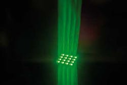
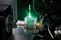
High-speed beam deflection is one option for fully utilizing the available laser power for USP microstructuring. To ensure high ablation quality with this method, the pulse energy is kept low. However, a high surface rate is obtained by virtue of a high pulse frequency coupled with a high scan speed. With a polygon scanner system developed at Fraunhofer ILT, it is possible to reach scan speeds of up to 350 m/s, enabling high-frequency laser pulses to be rapidly distributed onto large surfaces. Another option currently being pursued at Fraunhofer ILT is to split the laser beam into several beamlets, with significantly greater laser power. This beam splitting is made possible by a diffractive optical element (DOE). The research team at Fraunhofer ILT fitted the DOE between the beam source and a galvanometer scanner in such a way that the split laser beams are imaged in the galvanometer scanner. Focusing the beams using an f-theta lens eventually produces a periodic array of processing points, which can then be moved over the workpiece. This makes it possible to ablate patterns of any complexity.
Splitting the laser beam into 16 beamlets has been demonstrated at Fraunhofer ILT, where the workpiece is processed at 16 periodically arranged points simultaneously, resulting in a 16-fold increase in processing speed. In a laboratory experiment, experts have already successfully tested processing with 144 beamlets, and further scaling is possible.
This technology will permit the output reserves of current high-power USP laser systems to be fully utilized on the workpiece for laser processing. Processing times will drop accordingly, leading to a significant reduction in overall process costs. This will make USP lasers significantly more attractive to users from an economic point of view for manufacturing periodic microstructures. With this approach, it becomes economically feasible to structure even large surfaces. Fraunhofer ILT has developed a prototype machine for producing microstructures with USP lasers, which is to be further developed in future projects to make it suitable for industrial applications. The long-term goal is to use multi-100 W lasers for microstructuring before too long.
For further information contact: Stephen Eifel ([email protected]) or Dr. Jens Holtkamp ([email protected]).
Laser enhances skills in jewelry repair
Swindon, Wiltshire, UK-As the use of lasers for jewelry manufacturing and repair continues to grow, jewelers are now realizing their full potential. They are using this precision technology to undertake welding and joining processes that cannot be performed using traditional methods without risking damage to the precious metals or stones.
Deacon & Son (Swindon) Ltd was founded as a jewelers and watch and clock maker by George Deacon in 1848 and still remains a family-run business, now in its sixth generation. The catalyst for Deacon relocating to Swindon from his home town of Westbury can be linked to the Industrial Revolution and the arrival of the Great Western Railway in the town. The ambitious 26-year-old realized the need for time-keeping in this new environment, and the business was able to expand, winning one of the timing contracts for the railway on the line between Paddington and Swansea.
The company is now part of another revolution: the growing use of laser technology within jewelry workshops. The company's ongoing success and longevity can be attributed to a combination of dedication to quality, entrepreneurship, and the willingness to positively embrace innovation, exemplified in their use of laser technology for jewelry manufacture and repair.
Deacon & Son purchased a StarWeld Performance from Rofin-Baasel UK Ltd. some 5 years ago, and the laser, although not totally replacing the traditional soldering flame, has become the mainstay for jewelry repair here.
"The ability to be able to focus the beam so precisely and therefore produce only localized heat is a real benefit when working on intricate fretwork or in the close vicinity of delicate stones," explains Steve Davison of Deacon & Son. "Using the laser also means that we save significant amounts of time as we do not have to remove and then re-set stones when making repairs. This saving in time is a direct benefit to the customer as it reduces the cost."
The transition to laser is really quite straightforward, continues Davison. "The laser does not replace the craftsman skills that are essential in this industry, but actually enhances them through the precision and control available from the process. This in turn boosts confidence when undertaking some work that would be extremely difficult with the more traditional processes."
The laser here has clearly established itself as an integral part of this business and looks set to feature as a significant milestone in the company's illustrious history. There are a wide range of tasks where the use of laser technology brings significant benefits, including: repair to most types of jewelry, the ability to weld a wide range of sizes of jewelry pieces from larger castings to fine filigree wires, and repair or refill porosity in castings
Dave MacLellan of Rofin-Baasel says Starweld users benefit from a process of continuous improvement, which is based upon extensive customer feedback. The result is a system that inspires innovation and enhances the skills of the jeweler through precise control of the joining process.
For further information, contact [email protected]
UV laser for dicing and other micromachining applications
Santa Clara, CA - Coherent Inc. made news at the recent Photonics West Conference and Exhibition in San Francisco by highlighting a portfolio of picosecond products and short-pulse nanosecond lasers from its recent acquisitions of Lumera and Innolight, respectively. At the show, Coherent launched a completely new pulsed UV fiber laser, called Daytona, which the company claims fills an important gap in existing laser offerings. This is a seeded fiber-amplified laser that uses efficient frequency tripling to deliver 20 W of output at a wavelength of 355 nm, at adjustable pulsewidths as short as 1 ns and very high pulse repetition rates - up to 2 MHz.
"This new class of short-pulse, high rep rate nanosecond laser delivers several important benefits to users," said Victor David, product line manager at Coherent. "For example, it is the first micromachining laser to provide simple (i.e., software not hardware) adjustment of output pulsewidth over a broad range. Moreover the laser's design architecture is readily scalable to higher powers if and when applications demand this. Designed in response to market feedback, we're targeting this laser at fast scribing and dicing applications in semiconductor and solar, as well as some emerging applications involving ablative drilling and cutting of thin glass, where it can offer a higher quality process result with faster throughput when compared to existing lasers."
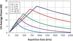
In terms of the operating regime, David explained that the new laser offers much higher repetition rates than is typical for nanosecond lasers. Daytona's power peaks at 1 MHz, depending on pulsewidth, and provides usable power at rates up to 2 MHz. David explains that this should enable drilling, scribing and dicing applications at faster scanning speeds in order to drive higher throughput. David also noted that, "In our applications laboratory and at beta site customers, we are seeing material removal rates comparable to nanosecond lasers, but routinely observing superior (heat-affected zone) HAZ characteristics."
However, it is the laser's variable pulsewidth that seemed most intriguing. Specifically, the pulsewidth can be adjusted continuously from 1 ns to 20 ns. As can be seen in the figure, decreasing the pulsewidth increases the peak output power, as expected, but also increases the average output power.
However, is the shortest pulsewidth always best? Not quite, in reality, said David. "In many cases, this delivers the optimum combination of high throughput and minimized HAZ. But, for example, when processing patterned wafers, these contain layers of different semiconductors, oxides and metals, and in practice, optimizing the cutting process involves subtle trade-offs. With its easy-to-vary pulsewidth, this laser's output can be varied to iteratively and quickly converge on the optimum settings for a particular job."
This flexibility will be particularly valuable for semiconductor packaging houses that process many different wafers from multiple foundries. They will be able to fine-tune the cutting conditions to deliver better results for their customers, commanding a premium price and doing this without requiring different, dedicated laser tools for each device/wafer, resulting in a faster ROI for the laser/tool.
"For integrated device manufacturers (IDMs), this flexibility can be an advantage. The back-end packaging lines are increasingly being used to process wafers from multiple front-end process lines and are being "re-tooled" more frequently for each device/node generation, with subtle differences in the wafer scribing/dicing characteristics," added David. "With this laser, scribing and dicing processes can be quickly optimized and dialed to a particular recipe, allowing the IDM or packaging house to process many different wafers on the same tool."
For further information, contact Victor David (victor.david@ coherent.com).
More Industrial Laser Solutions Current Issue Articles
More Industrial Laser Solutions Archives Issue Articles


