Provides users with precision, throughput, and CoO
Magnus Bengtsson, Dirk Müller, and Bernhard Klimt
More Industrial Laser Solutions Articles |
Picosecond lasers come of age for micromachining |
It has been known for some time that lasers with pulsewidths in the picosecond regime can offer significant advantages over longer pulse lasers for a wide variety of industrial microprocessing tasks. In particular, these benefits include virtually no heat affected zone, as well as the ability to work with an extremely broad range of materials, even those that are transparent in the visible and near-infrared. However, early picosecond lasers did not possess the necessary reliability, cost of ownership (CoO) and other practical characteristics required to make them feasible for use in many production environments. A new generation of industrial picosecond lasers has now emerged that provides the qualities needed to deliver on the promise of this technology. This article explores the principal differences between nanosecond and picosecond laser processing, reviews the basic architecture of currently available picosecond sources, and explores how they are being successfully used in industry today.
It has been known for some time that lasers with pulsewidths in the picosecond regime can offer significant advantages over longer pulse lasers for a wide variety of industrial microprocessing tasks.
Picosecond vs. nanosecond
The goal of micromachining is spatial selectivity, that is, the production of micron-scale features, such as holes and grooves, while avoiding peripheral thermal damage to surrounding material. In other words, the goal is precise, clean cuts with minimal heat affected zone (HAZ).
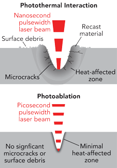
There are two basic mechanisms by which a laser can precision drill, scribe, or cut a material. Many traditional applications rely on infrared and visible Q-switched lasers, which have pulsewidths in the tens of nanoseconds range and which remove material via a photothermal interaction (see FIGURE 1). Here, the focused laser beam acts as a spatially confined, intense heat source. Targeted material is heated up rapidly, eventually causing it to be vaporized (essentially boiled away).
The advantage of this approach is that it enables rapid removal of relatively large amounts of target material (particularly considering the multi-kHz repetition rates at which Q-switched lasers typically operate). Furthermore, nanosecond laser technology is well established, and these sources are highly reliable and have attractive CoO characteristics. However, for the most demanding tasks, the size of the HAZ and the frequent presence of some recast material around the laser-produced feature, or delamination of surface coatings, can present a limitation.
The second mechanism for laser material removal is based on photoablation (FIGURE 1). Here, laser photons directly break the bonds holding the target material together, essentially atomizing it. This is a relatively cold process leading to less HAZ. Plus, it is very clean, leaving no recast material, with minimal need for post-processing.
The high energy of ultraviolet (UV) photons means that in many materials they can drive photoablation. Thus, Q-switched lasers with output in the UV remove material, at least to a certain extent, through photoablation. However, another way of achieving a purely photoablative interaction with a material is through the use of pulses in the picosecond domain or shorter. These ultrashort pulses allow for very high instantaneous peak powers (megawatts and above), and their high fluence drives multiphoton absorption, which excites electrons in the material and directly breaks atomic bonds (FIGURE 2). Moreover, because the pulsewidth is shorter than the thermal diffusion rate in the machined material, heat from residual thermal effects is largely removed with the atomized material before it can spread as a HAZ.
Besides producing effectively no HAZ, another major advantage of ultrafast processing is that it is compatible with a very broad range of materials, including several high bandgap materials (e.g., glass and certain polymers) that have low linear, optical absorption and hence are difficult to machine with existing, commercially available lasers. Specifically, the technique is "wavelength agnostic," that is, nonlinear absorption can be induced even if the material is normally transmissive at the laser wavelength.
Picosecond lasers are currently commercially available with output from the infrared to UV. Generally speaking, UV picosecond lasers deliver the best results in terms of high precision and minimal HAZ. This is because they operate in the most purely photoablative regime, and can also be focused to the smallest spot sizes (due to diffraction). On the other hand, infrared and visible picosecond lasers typically offer greater output powers, thus enabling higher throughput.
Picosecond laser architectures
While there is some diversity in the form and construction of commercially available, industrial, ultrafast lasers, they all utilize a certain basic configuration. Specifically, a passively mode-locked oscillator is used to generate output at pulsewidths of about 10 ps or shorter that are necessary to drive photoablation. However, most mode-locked oscillators produce relatively low energy pulses (in the nanojoule range) at repetition rates in the tens of MHz. This repetition rate is too high to be used with existing scanning technology, so a pulse picker is used to select a fraction of these pulses. The energy of these pulses is then boosted in an amplifier to produce the final output.
Most commercial picosecond products are based on one of the following architectures:
- a fiber laser oscillator followed by a fiber or rod type amplifier,
- a fiber laser oscillator followed by a free space amplifier, and
- a diode-pumped, solid-state oscillator followed by a free space amplifier.
The all-fiber (oscillator and amplifier) approach has the advantage of being relatively low cost and robust. A negative is that nonlinearities, scattering, and other effects in the fiber amplifier limit the maximum per pulse energy that can be attained to about 10 µJ (at a 10 ps pulsewidth). Thus, the only way of achieving high average power is by increasing the repetition rate. This poses practical difficulties with the beam delivery system because most beam deflection mechanisms, such as galvanometer scanners, are not fast enough to keep the individual pulses from overlapping at the work surface. For example, with a 50 µm diameter focused spot size and a pulse repetition rate of 1 MHz, the scanner velocity of a 50 m/s scanner would be required to avoid pulse overlap. Only a few scanners can deliver this rate of speed. The result is that process throughput becomes limited.
In order to achieve the higher pulse energies required for most applications, a fiber oscillator can be mated with a free space amplifier. This approach, for example, is utilized in Coherent's Talisker laser. Because of the relatively low energy output from the fiber seed, a regenerative amplifier is used. In a regenerative amplifier, a pulse undergoes a large number of passes and can therefore be amplified very substantially. Regenerative amplifiers also have the advantage of being compact and delivering good beam performance. Using this design, Talisker lasers can offer pulse energies of up to 180 µJ (at 1064 nm and 200 kHz).
The third approach is to use a diode-pumped, solid-state oscillator, which can produce higher pulse energies than a fiber seed. This is followed by a free-space amplifier, typically in either a regenerative or multipass configuration. In fact, more than one amplifier stage can be used to boost power to higher levels. For example, the products Coherent Inc. obtained through their acquisition of Lumera Laser GmbH in 2012 are based on a Nd:YVO4 seed, followed by one or more transient amplifiers, enabling the Lumera laser to reach pulse energies as high as 200 µJ (at 1064 nm). Table 1 summarizes the maximum average power that can be achieved with this flexible modular architecture when one, two, or three amplifier stages are used.
A transient multipass amplifier is used in this product line because it confers several other advantages in this situation. In particular, when compared to a regenerative amplifier, a transient amplifier offers the ability to reach higher repetition rates, as well as greater flexibility in terms of adjusting repetition rate (from single pulse to 2 MHz in this case).
Another extremely important benefit of the transient amplifier construction is that it supports "burst mode" operation in which the pulse picker is set to pass a string of consecutive pulses (typically up to 10) instead of just a single pulse. This entire pulse train is then amplified by the subsequent stages.
The advantage of burst mode is that, in some cases, it dramatically increases the ablation rate (the amount of material removed per unit time), for a given average laser power. For example, tests have shown a five to 10 times increase in ablation rate when a string of five pulses is sent through the amplifier instead of just single pulses (both at a 1 MHz repetition rate). The average power produced in each case is similar, and, in fact, the per pulse energy is lower in burst mode (since the amplifier gain is now spread over several pulses). However, the ablation rate does not seem to depend linearly upon pulse energy when the pulses are spaced so closely.
The exact mechanism for the ablation rate is still being investigated, but there are some favored theories emerging. It is thought that when there are only 20 ns or so between pulses, the material doesn't have time to relax and remains in a "preconditioned" state. This allows for subsequent pulses in the burst to achieve greater material removal despite their lower energy.
Burst mode expands the capabilities and opens up the parameter space of ultrafast micromachining substantially. It has proven most useful with materials having free electrons, such as steel, tungsten carbide, and silicon. Conversely, it provides little or no advantage with dielectrics such as ceramics and glass.
Reliable, industrial picosecond lasers
Most industrial users can only take advantage of the benefits of picosecond laser processing if it is delivered in the form of products with cost, reliability, and ease-of-use characteristics that are competitive with other laser, and even non-laser, based tools. Coherent, for example, employs design and construction practices to ensure this occurs in their products.
The first is a design in which there is substantial headroom, meaning an assembly that will perform properly even if some individual components deviate significantly from their nominal specifications. Furthermore, it guarantees that, even if changes occur in the product over time (such as decreases in mirror reflectivity or mechanical creep in optical mounts), that laser output will stay in specification.
Next, lasers are assembled from components that will avoid contamination within the laser cavity, in a cleanroom, and then hermetically sealed to prevent contaminants from entering.
Attention is also paid to mechanical design and the use of adjustable mounts, which might move over time, is minimized. Plus, every unit is shock-tested at over 100 g. If output power varies at all as a result of shock testing, the unit is failed, and the cause of the problem is determined.
Finally, these lasers are temperature controlled with a chiller to 0.1°C to ensure operational stability. Plus, the pump diodes are located in the power supply and fiber-coupled into the oscillator and amplifiers so as to eliminate any thermal loading from these sources.
The resulting reliability of these systems has been quite high. Customers have reported uptime of higher than 98%, even in 24/7 operating environments.
Typical applications
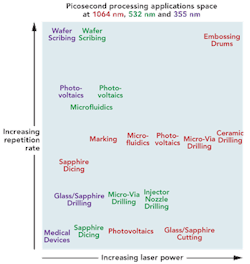
FIGURE 3 summarizes most of the key applications currently being serviced by picosecond lasers and indicates the wavelength, average power, and repetition rate regimes in which they operate.
An interesting emerging application for picosecond lasers is the cutting of thin glass used for smartphone displays. Laser processing offers advantages over mechanical methods for thin-glass cutting because it eliminates some of the post-processing finishing steps required for the latter. CO2 lasers have been successfully employed for thin-glass cutting, but are limited to cutting weakly strengthened glass and can't manage very thin glass very well. In one embodiment of ultrafast laser glass cutting, called filamentation cutting, the laser creates a string-like defect through the entire thickness of the substrate, thus allowing it to be easily separated. Filamentation cutting is advantageous because it can work with thicknesses from 50 µm to over 3 mm and can even be applied to certain types of strengthened glass.
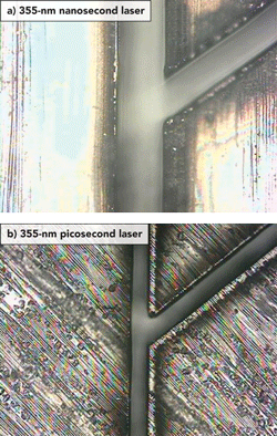
The picosecond laser has also been found useful for cutting thin metals. For example, PhotoMachining Inc., Pelham, NH, a supplier of high precision laser micromachining services and systems to the medical, aerospace, display, microelectronics and other industries, has used these systems in the production of medical implants. Typical materials for these industries are stainless steel, Hastelloy, Nitinol, and titanium. According to PhotoMachining CEO, Ronald Schaeffer, "We've been able to achieve extremely good edge quality without post-processing using a laser. With nanosecond lasers, we usually get some kind of melt on the cut edge which requires a subsequent electropolishing step to eliminate. We're typically producing features of about 25 µm in width on these products, so we use the 355 nm output in order to achieve the necessary spot size with a 100 mm focal length lens."
Another area where PhotoMachining has successfully employed picosecond laser processing is in structuring small, intricate parts made from carbon fiber reinforced polymer (CFRP). "These composites are made of woven fibers," notes Schaeffer, "and when you start cutting them they can change shape because internal stresses are relieved. If you add any heat to the process, then you've got a problem. We haven't found any nanosecond laser that can deliver the results that we need." In one particular application for an analytical instrument, Photomachining cut 30-µm-wide features in a 200-µm-thick CFRP part (FIGURE 4). Photomachining was able to consistently produce these features over the entire length of a 1-inch-diameter part without introducing significant distortion using a picosecond laser, again operating at 355 nm.
In terms of costs, the feature quality delivered by a picosecond laser, together with the ability to eliminate post-processing steps in many cases, make their operating rates competitive with many other laser and non-laser technologies. Consumables and operating costs are relatively small for this type of laser so CoO is dominated by the depreciation of the original purchase price. Table 2 summarizes the cost (per feature) that can be achieved with picosecond lasers for a number of common microprocessing tasks.
In conclusion, picosecond technology has now been productized so that practical sources are available with the cost, reliability, and operational characteristics necessary to make them useful in industrial settings. Taken together with lasers in the nanosecond and sub-nanosecond regime, this provides users with an extremely broad portfolio of capabilities in terms of precision, materials compatibility, throughput, and CoO. Successfully developing a new laser-based application is best accomplished by considering sources that cover this entire parameter space and partnering with someone who is experienced in laser microprocessing applications development. ✺
Magnus Bengtsson is director of strategic marketing at Coherent Inc., Dr. Dirk Müller is director of product line management at Lumera Laser Technology, Coherent, and Bernhard Klimt heads business development at Lumera Laser Technology, Coherent.
More Industrial Laser Solutions Current Issue Articles
More Industrial Laser Solutions Archives Issue Articles


